Display panel, array substrate and display device
A technology for array substrates and display panels, applied in instruments, nonlinear optics, optics, etc., can solve problems affecting the shading effect, and achieve the effects of avoiding light leakage, reducing manufacturing processes, and saving costs
- Summary
- Abstract
- Description
- Claims
- Application Information
AI Technical Summary
Problems solved by technology
Method used
Image

Examples
Embodiment 1
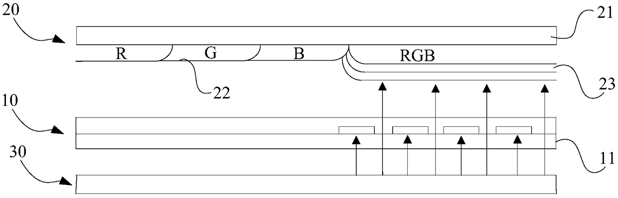
[0034] figure 2 It is a schematic structural diagram of a display panel provided in Embodiment 1 of the present invention, image 3 It is a schematic structural diagram of another display panel provided by Embodiment 1 of the present invention.
[0035] A display panel provided by the present invention includes an array substrate 10 and a color filter substrate 20 arranged opposite to the array substrate 10 , and a liquid crystal layer is arranged between the array substrate 10 and the color filter substrate 20 . Such as figure 2 As shown, the display panel includes an array substrate 10 , a color filter substrate 20 disposed opposite to the array substrate 10 , and a liquid crystal layer is further arranged between the array substrate 10 and the color filter substrate 20 .
[0036] Wherein, in this embodiment, the array substrate 10 includes a plurality of thin film transistors disposed on the first substrate 11, a plurality of first metal layers 12 arranged at intervals ...
Embodiment 2
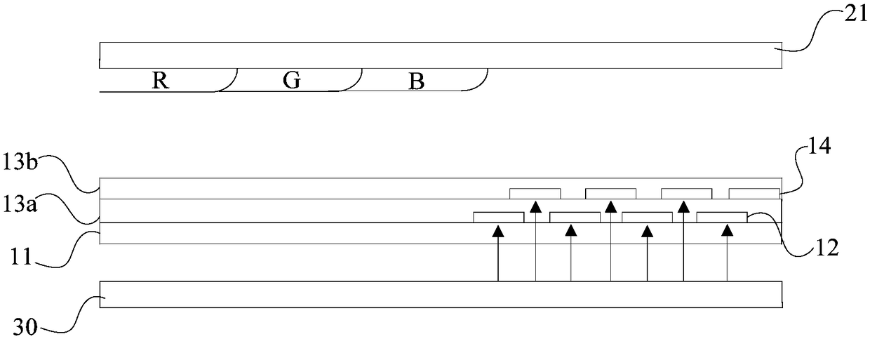
[0049] Figure 4 It is a schematic structural diagram of a display panel provided by Embodiment 2 of the present invention.
[0050] Further, on the basis of the above embodiments, in order to improve the display effect of the display panel, in this embodiment, the array substrate 10 further includes: a color filter layer 16 arranged on the display area of the first substrate 11, the color filter layer 16 The filter layer 16 includes a red filter layer, a green filter layer and a blue filter layer arranged in the same layer. The color filter layer 16 is an important component of the liquid crystal display panel. The color image of the liquid crystal display panel mainly depends on the color filter layer 16. In the traditional liquid crystal display panel, the color filter layer 16 is arranged on the color filter substrate 20. In the embodiment, the color filter layer 16 is arranged on the display area of the first substrate 11 of the array substrate 10, that is, the color...
Embodiment 3
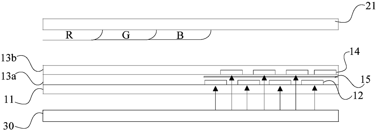
[0055] Figure 5 It is a schematic structural diagram of a display panel provided by Embodiment 3 of the present invention.
[0056] Further, on the basis of the first embodiment above, in this embodiment, the color filter substrate 20 includes a color filter layer 22 disposed on the second substrate 21 , and the second substrate 21 and the first color filter layer on the array substrate 10 A color-resist stack 23 is disposed at the corresponding position of the first metal layer 12 and the second metal layer 14 , and the color-resist stack 23 includes a stacked red filter layer, a green filter layer and a blue filter layer. The color filter substrate 20 includes a color filter layer 22 arranged on the second substrate 21. Specifically, the color filter layer 22 is arranged on the second substrate 21 at a position corresponding to the display area of the array substrate 10. The position corresponding to the first metal layer 12 and the second metal layer 14 on the array sub...
PUM
 Abstract
Description
Claims
Application Information
 - R&D
- Intellectual Property
- Life Sciences
- Materials
- Tech Scout
- Unparalleled Data Quality
- Higher Quality Content
- 60% Fewer Hallucinations
Browse by: Latest US Patents, China's latest patents, Technical Efficacy Thesaurus, Application Domain, Technology Topic, Popular Technical Reports.
© 2025 PatSnap. All rights reserved.Legal|Privacy policy|Modern Slavery Act Transparency Statement|Sitemap|About US| Contact US: help@patsnap.com