A kind of preparation method of msm photodetector

A photodetector and etching technology, applied in the fields of visible light and infrared detection and imaging, can solve problems such as difficult preparation, and achieve the effects of simplified preparation process, fast response speed, and small electrode spacing

Active Publication Date: 2020-04-10
UNIV OF ELECTRONICS SCI & TECH OF CHINA
View PDF5 Cites 0 Cited by
  • Summary
  • Abstract
  • Description
  • Claims
  • Application Information

AI Technical Summary

Problems solved by technology

This will make it very difficult to prepare an interdigitated electrode layer with a small electrode spacing on the surface of a semiconductor film integrated with a microstructure

Method used


Image

  • A kind of preparation method of msm photodetector
  • A kind of preparation method of msm photodetector
  • A kind of preparation method of msm photodetector

Examples


preparation example Construction

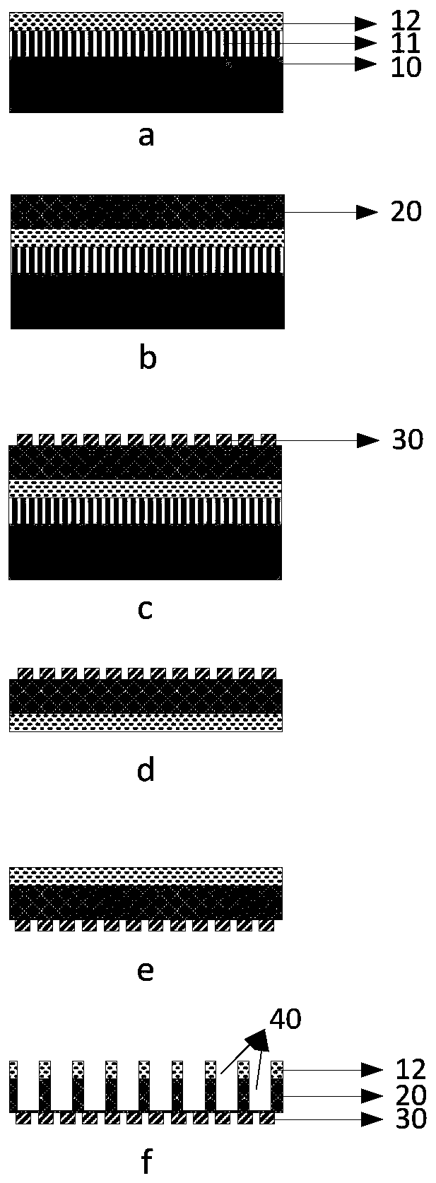
[0031] A kind of preparation method of MSM photodetector, comprises the following steps:

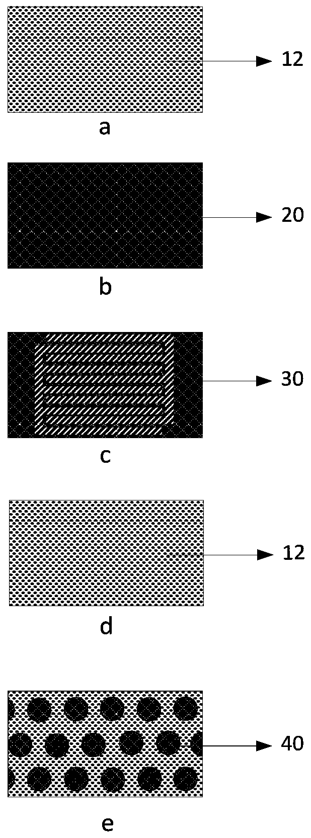
[0032](1) prepare semiconductor thin film 20 on SOI substrate; Wherein, SOI substrate comprises silicon substrate layer 10, silicon dioxide layer 11 and silicon thin film layer 12 that electroplating forms successively from bottom to top, as figure 1 -a with figure 2 As shown in -a, the semiconductor thin film 20 is adhered to the upper surface of the silicon thin film layer 12 by molecular beam epitaxy or metal organic chemical vapor deposition, as figure 1 -b with figure 2 -b shown;

[0033] (2) On the semiconductor thin film 20, adopt magnetron sputtering and patterning to form some interdigital electrodes 30, such as figure 1 -c with figure 2 -c shown;

[0034] (3) adopt buffered hydrofluoric acid solution to corrode silicon dioxide layer 11, make silicon dioxide layer 11 and silicon substrate layer 10 come off from silicon film layer 12, as figure 1 As shown in -d, the ...

Embodiment 1

[0039] Such as figure 1 Shown, a kind of preparation method of high-speed high-efficiency MSM photodetector comprises the steps:

[0040] (1) Select the SOI substrate as the device substrate. The SOI substrate includes a silicon substrate layer 10, a silicon dioxide layer 11 and a silicon thin film layer 12 formed by electroplating sequentially from bottom to top. In the SOI substrate, the silicon substrate layer is 500μm, the silicon dioxide layer thickness is 3μm, and the silicon film layer is 0.25μm. Clean the surface of the SOI substrate to remove contamination, and bake the SOI substrate at 200°C for 30 minutes to remove the water vapor on the surface. Such as figure 1 -a shown;

[0041] (2) Prepare a layer of silicon thin film on SOI substrate by molecular beam epitaxy method, the silicon thickness is 2 μm, such as figure 1 -b shown;

[0042] (3) A metal aluminum film is prepared on a silicon film by magnetron sputtering. The thickness of the film is 50nm. Several...

Embodiment 2

[0049] Such as figure 1 Shown, a kind of preparation method of high-speed high-efficiency MSM photodetector comprises the steps:

[0050] (1) Select the SOI substrate as the device substrate. The SOI substrate includes a silicon substrate layer, a silicon dioxide layer, and a silicon thin film layer formed by electroplating sequentially from bottom to top. The silicon substrate layer in the SOI substrate is 500 μm. The thickness of the silicon oxide layer is 3 μm, and the thickness of the silicon film layer is 0.25 μm. Clean the surface of the SOI substrate to remove contamination, and bake the SOI substrate at 200 ° C for 30 minutes to remove the moisture on the surface;

[0051] (2) Prepare a layer of silicon film on the SOI substrate by metal-organic chemical vapor deposition, and the thickness of the silicon film is 0.5 μm;

[0052] (3) An alloy film of metal bismuth and titanium was prepared on a silicon film by magnetron sputtering. The thickness of the film was 200nm....


PUM

PropertyMeasurementUnit
thicknessaaaaaaaaaa
thicknessaaaaaaaaaa
widthaaaaaaaaaa

Abstract

The invention discloses a method for preparing an MSM photodetector, which belongs to the technical field of photodetectors. The method for preparing a high-speed and high-efficiency MSM photodetector in the invention is as follows: in SOI(Si+SiO 2 +Si) semiconductor thin film was prepared on the substrate; interdigitated electrodes were prepared on the semiconductor thin film; SiO was removed by etching 2 layer, so that the device is separated from the silicon substrate; on the back of the device, the silicon and the semiconductor film are sequentially etched to form a periodic optical trap structure, and a high-speed and high-efficiency MSM photodetector is obtained. This preparation method integrates a periodic optical trap structure in the semiconductor film. While ensuring the response rate of the MSM photodetector, the photodetection efficiency of the detector is effectively improved, and the invention is used in visible light and infrared detection and imaging technologies.

Description

technical field [0001] The invention relates to the technical field of visible light and infrared detection and imaging, in particular to a preparation method of an MSM photodetector. Background technique [0002] Photo Detector (PD) is a key device for optical signal conversion in photoelectric detection system and optical fiber communication. At present, the ever-increasing speed of optical fiber communication systems puts forward higher and higher requirements on the response rate of photodetectors, and high-speed photodetectors have become an important research topic. Metal-Semiconductor-Metal Photo Detector (Metal-Semiconductor-Metal Photo Detector) or MSM-PD has gained wide attention and application due to its high responsivity, high sensitivity, simple structure, easy integration and low cost. [0003] MSM photodetector refers to the fabrication of metal electrodes on the surface of semiconductor materials to form back-to-back Schottky diodes, which are formed by the...

Claims


Application Information

Patent Timeline
Patent Type & Authority Patents(China)
IPC IPC(8): H01L31/18H01L31/108
CPCH01L31/1085H01L31/18Y02P70/50
Inventor 苟君牛青辰于贺王军蒋亚东
Owner UNIV OF ELECTRONICS SCI & TECH OF CHINA
Why Eureka
Try Eureka