Manufacturing method of silicon nitride dielectric layer, Josephson junction and superconducting quantum bit

A technology of silicon nitride medium and production method, which is applied in the field of superconducting quantum, can solve the problems of double-level defects, large microwave loss coefficient, and affecting the performance of superconducting qubits, so as to improve related performance, reduce microwave loss, reduce Effects of dual-level defects and magnetic impurities

Active Publication Date: 2019-01-29
SUZHOU INST OF NANO TECH & NANO BIONICS CHINESE ACEDEMY OF SCI
View PDF3 Cites 6 Cited by
  • Summary
  • Abstract
  • Description
  • Claims
  • Application Information

AI Technical Summary

Problems solved by technology

Generally, each superconducting qubit includes at least one Josephson junction, and the Josephson junction is a weakly coupled tunnel junction formed by embedding a dielectric layer film between two superconductors, wherein the prior art generally uses aluminum oxide (AlO X ) amorphous material to make the dielectric layer of the Josephson junction, and the microwave loss coefficient of alumina amorphous material is about 1.6×10 -3 , its microwave loss coefficient is large, and it is easy to introduce dual-level defects and magnetic impurities, which seriously affects the performance of superconducting qubits and affects the application of superconducting qubits in the field of microwave engineering technology

Method used


Image

  • Manufacturing method of silicon nitride dielectric layer, Josephson junction and superconducting quantum bit
  • Manufacturing method of silicon nitride dielectric layer, Josephson junction and superconducting quantum bit
  • Manufacturing method of silicon nitride dielectric layer, Josephson junction and superconducting quantum bit

Examples


Embodiment Construction

[0021] In order to make the object, technical solution and advantages of the present invention clearer, the specific implementation manners of the present invention will be described in detail below in conjunction with the accompanying drawings. Examples of these preferred embodiments are illustrated in the accompanying drawings. The embodiments of the invention shown in and described with reference to the drawings are merely exemplary, and the invention is not limited to these embodiments.

[0022] Here, it should also be noted that, in order to avoid obscuring the present invention due to unnecessary details, only the structures and / or processing steps that are closely related to the solution according to the present invention are shown in the drawings, and the relationship between them is omitted. Little other details.

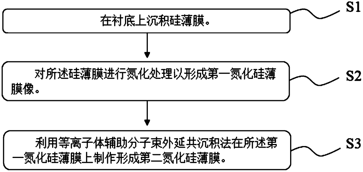
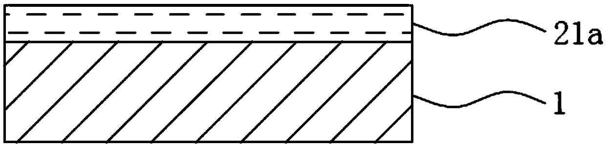
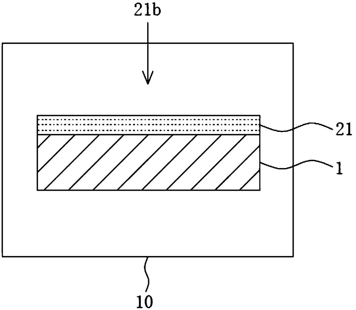
[0023] refer to figure 1 As shown, this embodiment provides a silicon nitride (SiN X ) The method for making the dielectric layer, comprising:

[0024]...


PUM


Abstract

The invention discloses a manufacturing method of a silicon nitride dielectric layer, a Josephson junction and a superconducting quantum bit. The manufacturing method of the silicon nitride dielectriclayer comprises the steps of depositing a silicon film on a substrate; carrying out nitridation processing on the silicon film to form a first silicon nitride film; and manufacturing a second siliconnitride film on the first silicon nitride film by using a plasma assisted molecular beam epitaxial codeposition method. According to the method, the dielectric layer is manufactured by using the silicon nitride material with a low microwave loss coefficient, so that the microwave loss of the dielectric layer is reduced. Meanwhile, in the superconducting quantum bit of the silicon nitride dielectric layer manufactured based on the method, the silicon nitride material can be adopted to manufacture a protective layer of the superconducting quantum bit, thereby effectively reducing double energylevel defects and magnetic impurities introduced by the surface interface, and being conducive to improving related performance of the Josephson junction and the superconducting quantum bit. In addition, the manufacturing method of the silicon nitride dielectric layer can obtain the high-performance silicon nitride dielectric layer under a technological condition with low requirements, thereby being conducive to mass production.

Description

technical field [0001] The invention relates to the field of superconducting quantum technology, in particular to a manufacturing method of a silicon nitride dielectric layer, a Josephson junction and a superconducting qubit. Background technique [0002] The basic unit of a quantum computer is the qubit. Among them, the superconducting qubit is compatible with the traditional semiconductor microfabrication process. Its manipulation and measurement involve microwave engineering technology, and its research progress is ahead of other quantum computing research directions. Generally, each superconducting qubit includes at least one Josephson junction, and the Josephson junction is a weakly coupled tunnel junction formed by embedding a dielectric layer film between two superconductors, wherein the prior art generally uses aluminum oxide (AlO X ) amorphous material to make the dielectric layer of the Josephson junction, and the microwave loss coefficient of alumina amorphous mat...

Claims


Application Information

Patent Timeline
Patent Type & Authority Applications(China)
IPC IPC(8): H01L21/02H01L39/22
CPCH01L21/0217H01L21/02247H01L21/02269H10N60/12
Inventor 冯加贵武彪熊康林孙骏逸黄永丹郑明昊丁孙安陆晓鸣
Owner SUZHOU INST OF NANO TECH & NANO BIONICS CHINESE ACEDEMY OF SCI
Why Eureka
Try Eureka