Color film substrate, preparation method thereof and quantum dot display device comprising same

A color film substrate and color film layer technology, which is applied in identification devices, nonlinear optics, optics, etc., can solve the problem of large gaps between flat materials and black embankments, unfavorable nano-imprinting to form gratings, and inability to completely erase step differences, etc. problems, to achieve the effect of commercialization

Active Publication Date: 2019-02-01
BOE TECH GRP CO LTD
View PDF17 Cites 14 Cited by
  • Summary
  • Abstract
  • Description
  • Claims
  • Application Information

AI Technical Summary

Problems solved by technology

[0003] In the existing process of preparing quantum dot display devices, it is necessary to planarize the substrate substrate after completing the green light quantum dot material (QD G) and the red light quantum dot material (QD R), but due to the flat material and the black bank (bank) and There is a large gap between the color resists, and the level difference cannot be completely erased after planarization. This structure with a low pixel area and high sides is not conducive to the formation of gratings by nanoimprinting.

Method used


Image

  • Color film substrate, preparation method thereof and quantum dot display device comprising same
  • Color film substrate, preparation method thereof and quantum dot display device comprising same
  • Color film substrate, preparation method thereof and quantum dot display device comprising same

Examples


Embodiment Construction

[0034] Example embodiments will now be described more fully with reference to the accompanying drawings. Example embodiments may, however, be embodied in many forms and should not be construed as limited to the embodiments set forth herein; rather, these embodiments are provided so that this disclosure will be thorough and complete, and will fully convey the concept of example embodiments to those skilled in the art. In the drawings, the thickness of regions and layers are exaggerated for clarity. The same reference numerals in the drawings denote the same or similar structures, and thus their detailed descriptions will be omitted.

[0035] It should be noted that terms such as upper and lower in the present invention are only relative concepts or refer to the state of the product in the process, and should not be regarded as limiting.

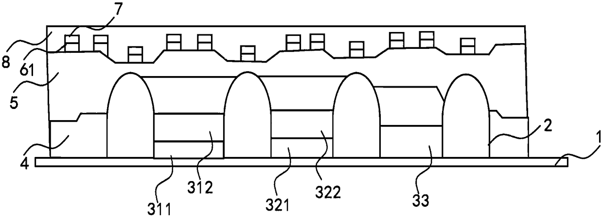
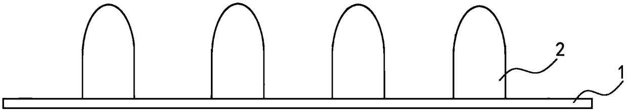
[0036] Such as figure 1 As shown, the color filter substrate includes a base substrate 1 , a black matrix, a color filter layer, a first p...


PUM


Abstract

The invention provides a color film substrate. The color film substrate comprises a substrate body, a black matrix, a color film layer, a first planarization layer, a second planarization layer, a grating layer and a third planarization layer, wherein the black matrix is formed on the substrate body and comprises a plurality of openings and a bank part which surrounds the openings and forms a plurality of pixel areas, and the bank part comprises a black dye; the color film layer is formed in each opening and comprises a color quantum dot material layer formed in at least part of the opening regions; the first planarization layer covers the color film layer, and the bank part is exposed out of the first planarization layer; the second planarization layer covers the first planarization layerand the bank part, and the distance between the surface, relative to the surface of the first planarization layer and corresponding to the bank part, of the second planarization layer and the substrate body is smaller than the distance between the surface, corresponding to the pixel areas, of the second planarization layer and the substrate body; the grating layer is formed on the second planarization layer; the third planarization layer covers the grating layer. According to the substrate, the planarization layers with the high pixel areas and low black bank areas are formed so that nano-grating of the pixel areas can be well formed.

Description

technical field [0001] The invention relates to the technical field of quantum dot display, and in particular to a color filter substrate, a preparation method thereof, and a quantum dot display device containing the same. Background technique [0002] With the rapid development of the display field, quantum dot display technology has attracted more and more attention due to its unique luminous properties, excellent stability, wider color gamut coverage, and relatively low cost. Currently, in a display device using quantum dot display technology, the blue light emitted by the backlight is usually used to excite the quantum dot material to emit red light and green light, thereby providing color display. [0003] In the existing process of preparing quantum dot display devices, it is necessary to planarize the substrate substrate after completing the green light quantum dot material (QD G) and the red light quantum dot material (QD R), but due to the flat material and the blac...

Claims


Application Information

Patent Timeline
Patent Type & Authority Applications(China)
IPC IPC(8): G09F9/00G02F1/1333G02F1/1335
CPCG02F1/1333G02F1/133504G09F9/00G02F1/133357G02F1/133512G02F1/133514G02F1/133617G02F2202/36G02F1/133548G02F1/133516G02F1/133528
Inventor 岳阳舒适徐传祥黄海涛李翔卢江楠姚琪
Owner BOE TECH GRP CO LTD
Why Eureka
Try Eureka