
Patsnap Eureka
For R&D, Patsnap Eureka makes reading and utilizing patents & technical documents easy.
Patsnap Eureka AIR
Designed for self-driven R&D workflows. Generate viable solutions, solve complex R&D challenges, empower your innovation with AI.

Patsnap Eureka Materials
Designed for material experts only. Revolutionize your material R&D, from search, analyze, to developing new materials.

TechResearch
Generate reliable direction feasibility study reports for your R&D in just a few steps.

TechSeek
Discover and master advanced knowledge NOW. Basics, ideas, possibilities, all at once.

TechMind
As an expert in R&D Theories, TechMind can generates customized viable solutions instantly.

TechRisk
Analyze your overall solution with one click, know your potential R&D risks in advance.

TechMonitor
Get weekly tech updates, stay abreast of the latest tech innovations and key insights.
3D-NAND flash memory formation method
A 3D-NAND, flash memory technology, applied in electrical components, electric solid state devices, circuits, etc., can solve the problems of poor performance of 3D-NAND flash memory, and achieve the effect of reducing process costs and process steps
- Summary
- Abstract
- Description
- Claims
- Application Information
AI Technical Summary
Problems solved by technology
Method used
Image

Examples
Embodiment Construction
[0022] As mentioned in the background, the performance of the prior art 3D-NAND flash memory is poor.
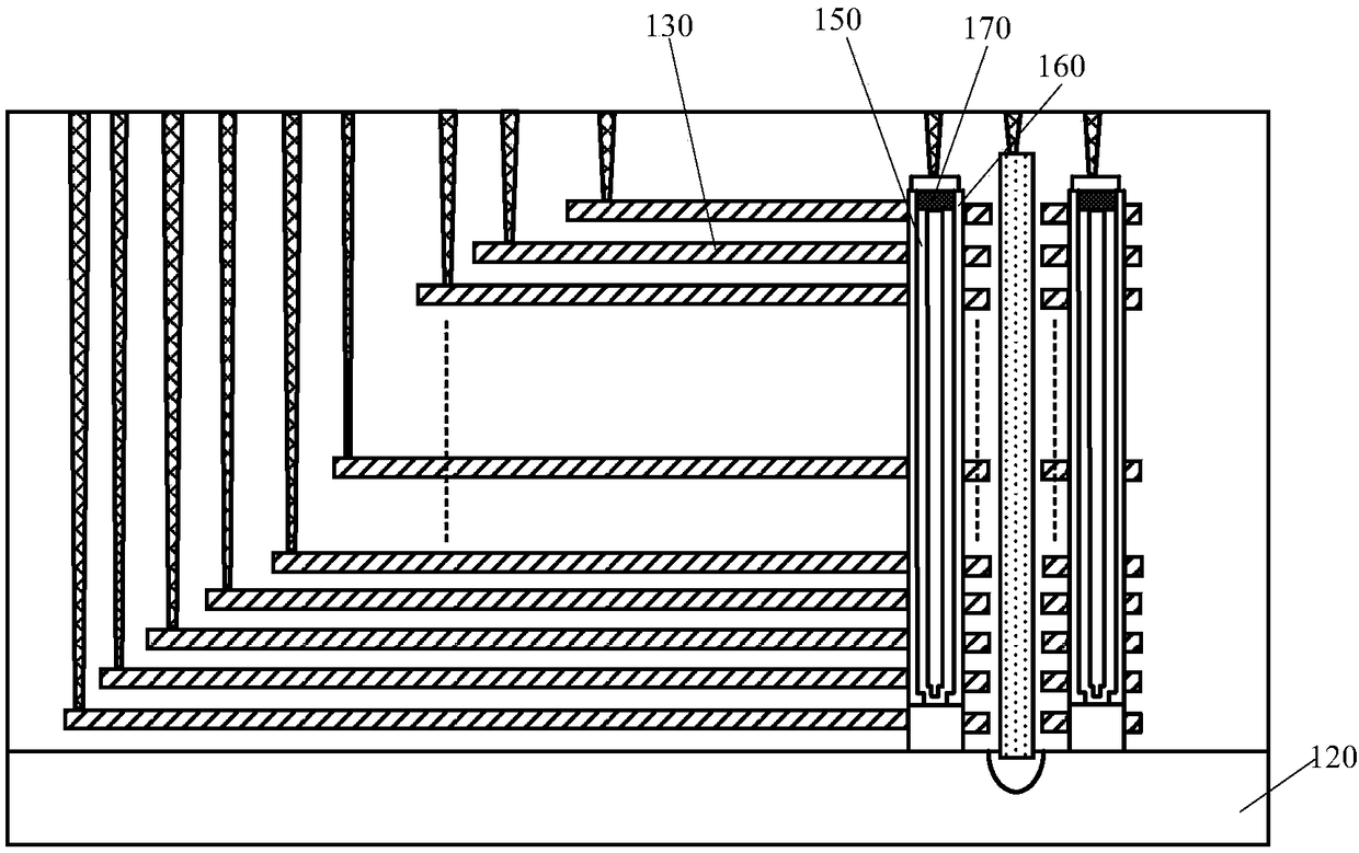
[0023] A kind of 3D-NAND flash memory, the type of 3D-NAND flash memory is N type, refer to figure 1 3D-NAND flash memory includes: a semiconductor substrate 120; a stacked structure on the semiconductor substrate 120, the stacked structure includes cross-stacked insulating layers and control gates 130; a channel structure running through the stacked structure, the trench The channel structure includes a channel layer 150 and a memory layer 160 extending in a direction perpendicular to the surface of the semiconductor substrate 120, and the memory layer 160 includes a blocking dielectric layer, a storage layer and a tunneling dielectric layer; located in the top region of the channel structure N-type drain doped region 170.
[0024] There are two main ways to perform erasing operations in 3D-NAND, one is substrate bulk erasing, and the other is GIDL (gate induced drain leak...
PUM
 Abstract
Description
Claims
Application Information
 - R&D Engineer
- R&D Manager
- IP Professional
- Industry Leading Data Capabilities
- Powerful AI technology
- Patent DNA Extraction
Browse by: Latest US Patents, China's latest patents, Technical Efficacy Thesaurus, Application Domain, Technology Topic, Popular Technical Reports.
© 2024 PatSnap. All rights reserved.Legal|Privacy policy|Modern Slavery Act Transparency Statement|Sitemap|About US| Contact US: help@patsnap.com