Substrate integrated gap waveguide coupler design method

A technology of substrate integration and gap waveguide, which is applied in the field of electronics, can solve problems such as no public reports, and achieve the effects of easy integration, high isolation, and low profile

Inactive Publication Date: 2019-02-01
YUNNAN UNIV
View PDF2 Cites 6 Cited by
  • Summary
  • Abstract
  • Description
  • Claims
  • Application Information

AI Technical Summary

Problems solved by technology

[0008] Contents of the present invention, through literature search, do not see the public report identical with the present invention

Method used


Image

  • Substrate integrated gap waveguide coupler design method
  • Substrate integrated gap waveguide coupler design method
  • Substrate integrated gap waveguide coupler design method

Examples


Embodiment Construction

[0044] specific implementation plan

[0045] The technical solutions of the present invention will be further described in detail below in conjunction with specific embodiments.

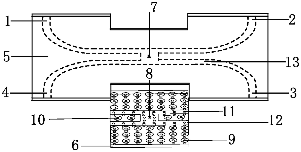
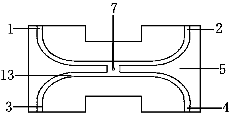
[0046] Such as Figure 1-5 As shown, a design method of a substrate-integrated gap waveguide coupler, including: an upper dielectric plate (5), a lower dielectric plate (6), wherein:

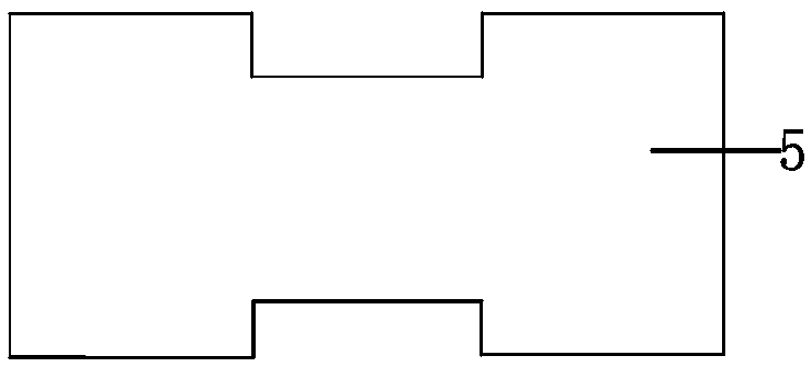
[0047] a. The upper dielectric plate (5) is the gap layer of the substrate-integrated gap waveguide. It is a rectangular dielectric plate with two rectangular slots. The upper surface is printed with a metal ground, and the lower surface is printed with a coupled microstrip line (13) ; There is a rectangular first slit (7) in the middle of the coupled microstrip line (13); the four ports of the coupled microstrip line (13) are respectively the first port (1), the second port (2), and the second port (2). Three ports (3) and the fourth port (4); the first port (1) is an input port, the second port (2) is a through por...


PUM


Abstract

The invention relates to a substrate integrated gap waveguide coupler design method. A coupler structure is formed by the close connection of an upper dielectric plate (5) and a lower dielectric plate(6). The upper surface of the upper dielectric plate (5) is provided with a grounding metal layer through printing, and the lower surface of the upper dielectric plate (5) is provided with a couplingmicrostrip line (13) through printing. The upper surface of the lower dielectric plate (6) is provided with an H-shaped coupling microstrip line (12) through printing, and the H-shaped coupling microstrip line (12) and a metal via hole (11) form an H-bridge transmission ridge. Two sides of the H-bridge transmission ridge are each provided with a first EBG structure array (9), and the center of the H-bridge transmission ridge is provided with a second EBG structure array (10), wherein the lower surface is printed with a metal layer. The method provided by the invention is improved from the theoretical basis of a microstrip branch line coupler. The waveguide coupler is easy for integration, is small in size, is wide in bandwidth, is small in loss, and is higher in isolation degree.

Description

technical field [0001] The invention relates to the field of electronic technology, in particular to a design method for a substrate-integrated gap waveguide coupler. Background technique [0002] Directional coupler is an important microwave and millimeter wave device, which can be used for signal isolation, separation and mixing, such as power monitoring, source output power stabilization, signal source isolation, frequency sweep test of transmission and reflection, etc. The forms of couplers mainly include waveguide couplers and microstrip couplers. With the development of communication systems, the frequency requirements for microwave and millimeter wave devices are getting higher and higher. However, traditional rectangular waveguide couplers and microstrip couplers have large losses at high frequencies, which limits their application at high frequencies. [0003] The emergence of Substrate Integrated Waveguide (SIW) has solved the above problems well. Substrate Integr...

Claims


Application Information

Patent Timeline
Patent Type & Authority Applications(China)
IPC IPC(8): H01P5/16
CPCH01P5/16
Inventor 王珂申东娅张秀普
Owner YUNNAN UNIV
Why Eureka
Try Eureka