Supercharge Your Innovation With Domain-Expert AI Agents!

Microelectromechanical systems and method of manufacturing the same

一种微机电系统、电子装置的技术,应用在电视系统的零部件、发电机/电动机、微电子微观结构装置等方向,能够解决影响MEMS压力传感器性能、MEMS裸片倾斜、降低MEMS裸片性能等问题

Active Publication Date: 2019-02-05
ADVANCED SEMICON ENG KOREA INC
View PDF4 Cites 0 Cited by
  • Summary
  • Abstract
  • Description
  • Claims
  • Application Information

AI Technical Summary

Problems solved by technology

However, due to the inconsistent diameter of the solder balls, the MEMS die may tilt, which may degrade the performance of the MEMS die
Additionally, adhesive applied between the MEMS die and the substrate can flow into the sensing opening (through the substrate), which can also affect the performance of the MEMS pressure sensor

Method used


Image

  • Microelectromechanical systems and method of manufacturing the same
  • Microelectromechanical systems and method of manufacturing the same
  • Microelectromechanical systems and method of manufacturing the same

Examples


Embodiment Construction

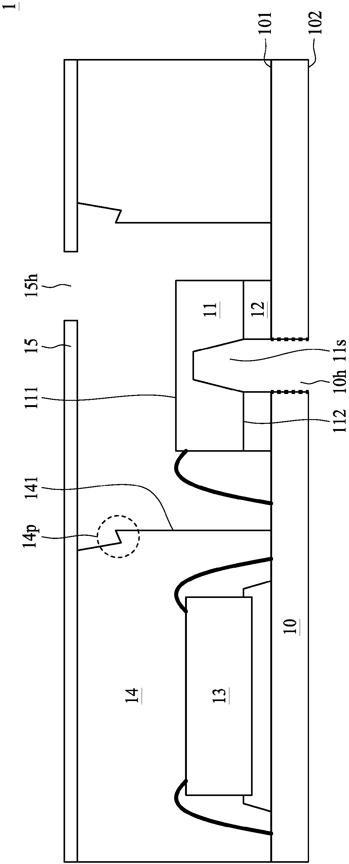
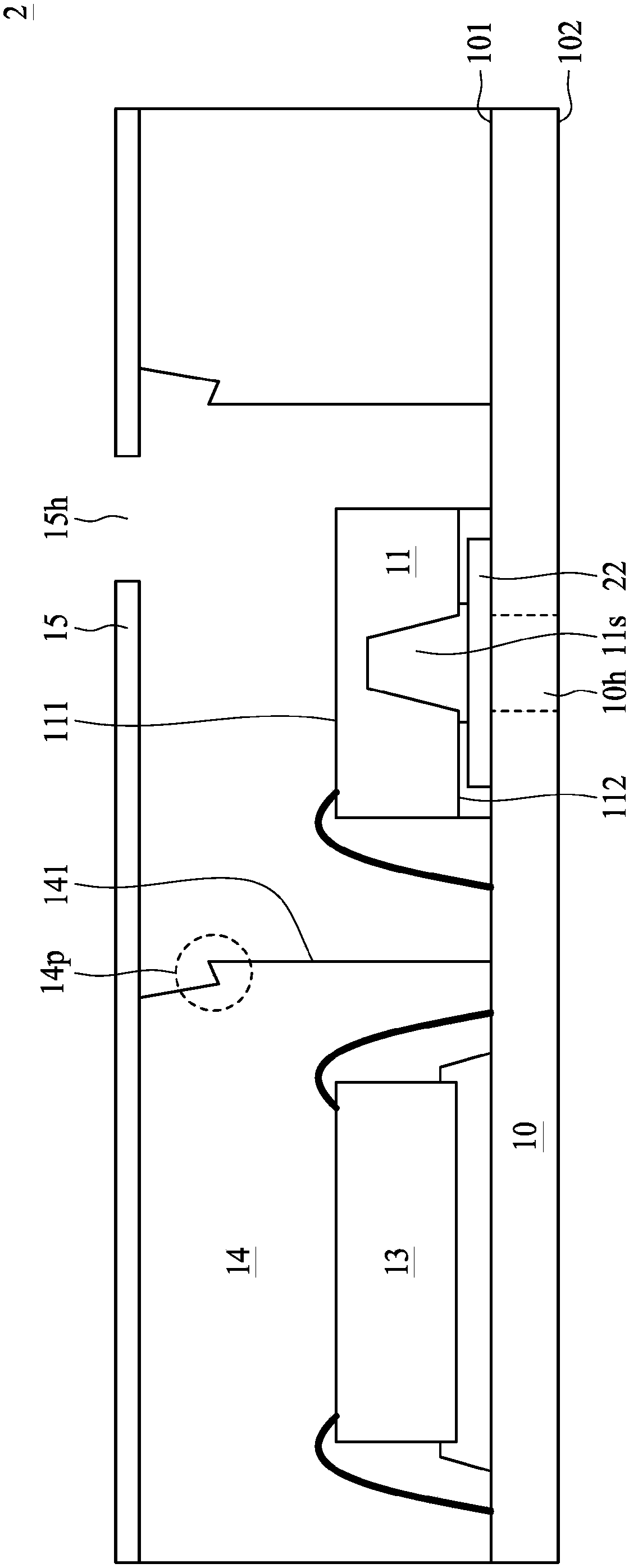
[0019] Figure 1A A semiconductor package device 1 according to some embodiments of the present disclosure is explained. The semiconductor package device 1 includes a substrate 10 , a MEMS device 11 (or simply MEMS 11 ), an attachment element 12 , an electronic device 13 , a package body 14 and a metal cover 15 .

[0020] The substrate 10 can be, for example, a printed circuit board (PCB), a copper foil laminate such as paper, a composite copper foil laminate, a polymer-impregnated fiberglass-like copper foil laminate, or two or more thereof. combination. Substrate 10 may include interconnect structures such as redistribution layers (RDL) or ground elements. The substrate 10 has a surface 101 and a surface 102 opposite to the surface 101 . In some embodiments, surface 101 of substrate 10 is referred to as a top surface or first surface, and surface 102 of substrate 10 is referred to as a bottom surface or second surface. The substrate 10 defines an opening 10h through the s...


PUM


Abstract

The present disclosure relates to an electronic device. The electronic device comprises a substrate, a micro-electromechanical systems (MEMS) device and an attachment element. The substrate defines anopening penetrating the substrate. The MEMS device has an active surface facing away from the substrate and a sensing region facing toward the opening. The attachment element is disposed on the substrate and surrounding the opening and the sensing region of the MEMS device.

Description

technical field [0001] The present disclosure relates to a semiconductor package device including a micro-electro-mechanical system (MEMS) and a manufacturing method thereof. Background technique [0002] MEMS (as used herein, the term "MEMS" can be used to refer to a single microelectromechanical system or multiple microelectromechanical systems) can be used in semiconductor devices to detect signals (e.g., sound, motion or motion, pressure, gas, humidity, temperature etc.) and converting the detected signal into an electrical signal. Semiconductor devices (eg, semiconductor devices using MEMS) have gradually become more complex. This trend is driven at least in part by the need for smaller sizes and enhanced processing speeds. At the same time, there is a demand for further miniaturization of many electronic products incorporating these semiconductor devices. In some cases it may be desirable to reduce the space occupied by MEMS on the substrate of a semiconductor devic...

Claims


Application Information

Patent Timeline
Patent Type & Authority Applications(China)
IPC IPC(8): B81B7/00B81B7/02
CPCB81B7/0006B81B7/0048B81B7/02B81B7/0061B81B2201/0257B81C3/001H01L23/02H01L29/84
Inventor 裴栒兴尹皓权薛庆焕金德泳
Owner ADVANCED SEMICON ENG KOREA INC
Features
  • R&D
  • Intellectual Property
  • Life Sciences
  • Materials
  • Tech Scout
  • Unparalleled Data Quality
  • Higher Quality Content
  • 60% Fewer Hallucinations
Learn More