Embedded touch control array substrate, display panel and liquid crystal display device

An array substrate and embedded technology, applied in nonlinear optics, instruments, optics, etc., can solve the problems of unfavorable narrow bezel design and affecting the width of the bezel, and achieve the effect of realizing narrow bezel design requirements and saving space

Pending Publication Date: 2019-02-12
KUSN INFOVISION OPTOELECTRONICS
View PDF6 Cites 7 Cited by
  • Summary
  • Abstract
  • Description
  • Claims
  • Application Information

AI Technical Summary

Problems solved by technology

[0004] However, in the production process of the product, it was found that the data lines in the array substrate and the touch lines that lead out to multiple block electrodes in the common electrode cover most of the fan-out area. Take the resolution of full HD as an example: the array The fan-out wires of the source side data lines in the substrate need 720*3 wires. When the touch wires are added, 1 / 3 of the fan-out wires are added. At this time, 720*4 metal wires are required, which will affect the The width of the frame (lower frame) on the source side is not conducive to the realization of narrow frame design

Method used


Image

  • Embedded touch control array substrate, display panel and liquid crystal display device
  • Embedded touch control array substrate, display panel and liquid crystal display device
  • Embedded touch control array substrate, display panel and liquid crystal display device

Examples


Embodiment Construction

[0021] In order to further explain the technical means and effects of the present invention to achieve the intended purpose of the invention, the specific implementation, structure, features and effects of the present invention will be described in detail below in conjunction with the accompanying drawings and examples.

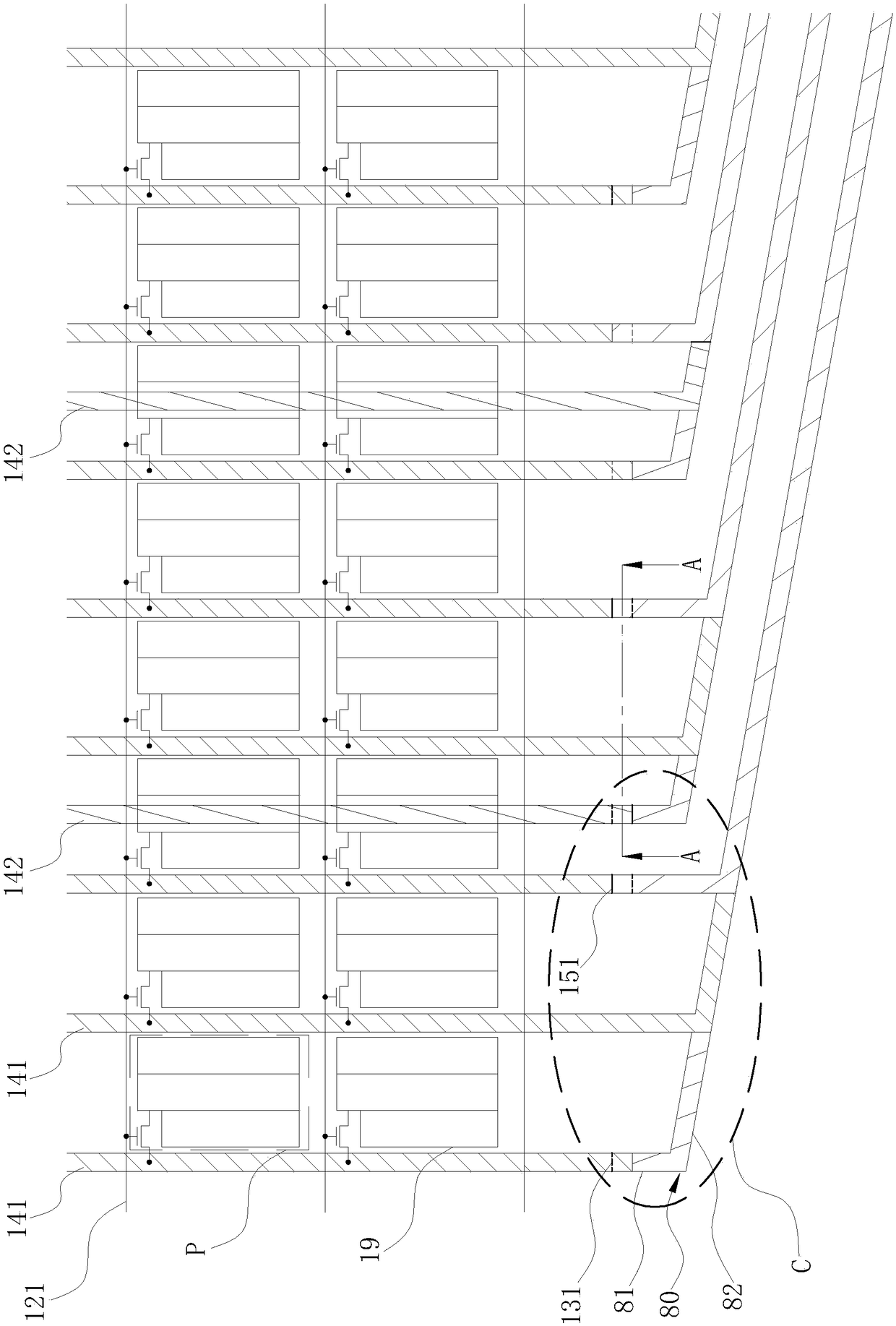
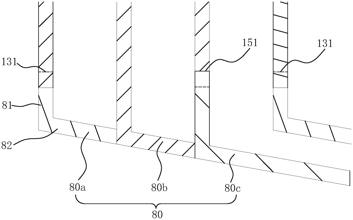
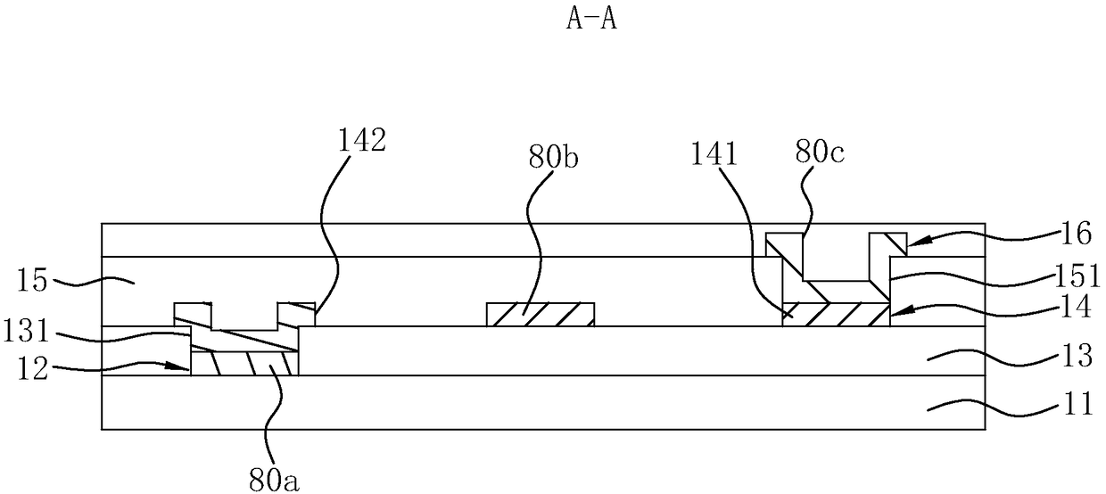
[0022] figure 1 is a schematic structural diagram of the fan-out area in the embodiment of the present invention, figure 2 for figure 1 The enlarged schematic diagram of the dotted box C in the middle, image 3 for figure 1 A schematic cross-sectional view along line A-A, Figure 4 It is a schematic plan view of the array substrate in the embodiment of the present invention. Such as Figure 1 to Figure 4 As shown, the embodiment of the present invention provides an in-cell touch array substrate, which has a display area 100 and a non-display area. The non-display area includes a fan-out area 200. The in-cell touch array substrate includes a substrate 11...


PUM


Abstract

The invention discloses an embedded touch control array substrate, a display panel and a liquid crystal display device. The embedded touch control array substrate is provided with a display area and afan-out area and comprises an underlayment and further comprises a first metal layer, a second metal layer and a third metal layer which are sequentially arranged along the underlayment from bottom to top, and insulation layers are arranged between the metal layers; the first metal layer is provided with scanning lines in the display area and provided with first leads in the fan-out area; the second metal layer is provided with data lines and touch control lines in the display area and provided with second leads in the fan-out area; the third metal layer is provided with third leads in the fan-out area; and every adjacent three of the first leads, the second leads, the third leads serve as one set in the fan-out area, each set of three leads comprises the corresponding first lead, the corresponding second lead and the corresponding third lead, each set of three leads is located at different layers, the vertical projections of each set of three leads in the array substrate are overlapped, each lead is used for being connected with the corresponding data line or touch control line, and the thickness of a lower frame of the array substrate can be decreased.

Description

technical field [0001] The invention relates to the field of display technology, and in particular to an in-cell touch array substrate, a display panel and a liquid crystal display device. Background technique [0002] With the rapid development of display technology, touch screens (touch panels) have pervaded all aspects of people's lives. With the continuous advancement of touch technology, people have higher and higher requirements for touch products. While paying attention to sensitivity, lightness and thinness must also be considered, which has greatly increased the manufacturing cost of display panel manufacturers. [0003] At present, touch screens can be classified into: on-cell touch panels and in-cell touch panels according to their composition and structure. In the embedded touch screen, the touch electrodes of the touch screen are embedded inside the display screen, for example, the touch electrodes are embedded on the array substrate. One of the methods is to ...

Claims


Application Information

Patent Timeline
Patent Type & Authority Applications(China)
IPC IPC(8): G02F1/1362G02F1/1333
CPCG02F1/13338G02F1/136286G02F1/13629
Inventor 刘厚锋魏祥利王芳
Owner KUSN INFOVISION OPTOELECTRONICS
Why Eureka
Try Eureka