Pixel arrangement structure, display panel and display device

A technology of pixel arrangement and display panel, applied in semiconductor devices, electrical components, circuits, etc., can solve problems such as improving pixel aperture ratio, achieve the effect of improving product yield and ensuring luminous effect

Active Publication Date: 2019-02-12
KUNSHAN GO VISIONOX OPTO ELECTRONICS CO LTD
View PDF8 Cites 6 Cited by
  • Summary
  • Abstract
  • Description
  • Claims
  • Application Information

AI Technical Summary

Problems solved by technology

[0006] The embodiment of the present application provides a pixel arrangement structure, which is used to solve the problem in the prior art that the aperture ratio of pixels cannot be effectively increased while ensuring the reduction of the aperture area of ​​the evaporation mask.
[0007] The embodiment of the present application provides a display panel, which is used to solve the problem in the prior art that the aperture ratio of pixels cannot be effectively increased while ensuring the reduction of the aperture area of ​​the evaporation mask.
[0008] The embodiment of the present application also provides a display device, which is used to solve the problem in the prior art that the aperture ratio of pixels cannot be effectively increased while ensuring the reduction of the aperture area of ​​the evaporation mask.

Method used


Image

  • Pixel arrangement structure, display panel and display device
  • Pixel arrangement structure, display panel and display device
  • Pixel arrangement structure, display panel and display device

Examples


Embodiment Construction

[0040] In order to make the purpose, technical solution and advantages of the present application clearer, the technical solution of the present application will be clearly and completely described below in conjunction with specific embodiments of the present application and corresponding drawings. Apparently, the described embodiments are only some of the embodiments of the present application, rather than all the embodiments. Based on the embodiments in this application, all other embodiments obtained by persons of ordinary skill in the art without making creative efforts belong to the scope of protection of this application.

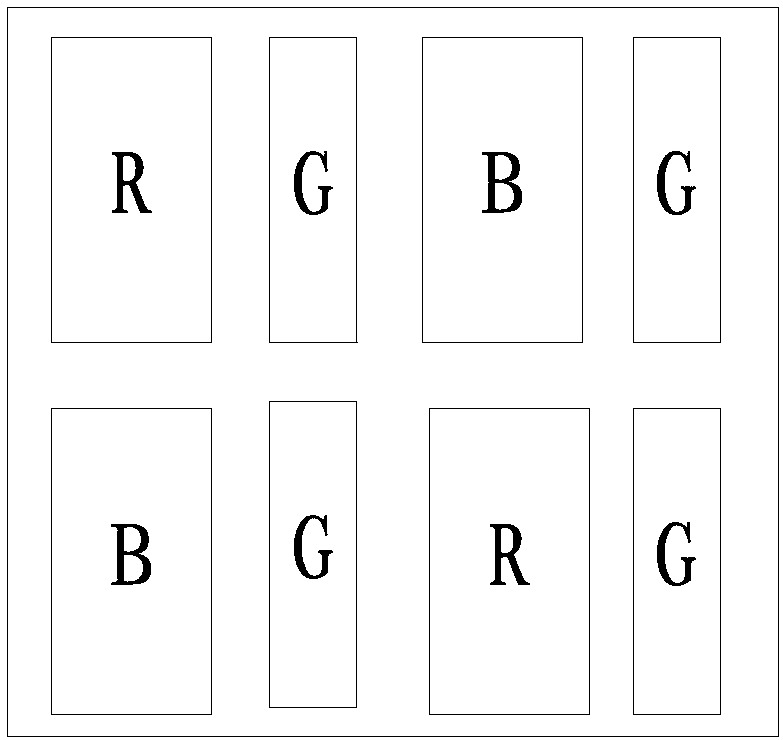
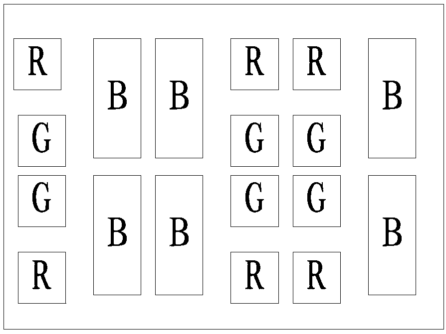
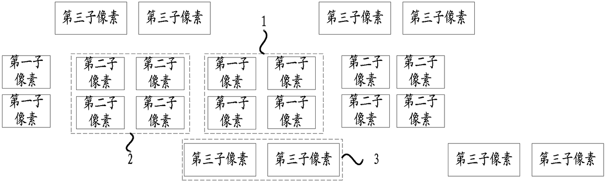
[0041] Such as image 3 As shown, a pixel arrangement structure provided by the embodiment of the present application. The pixel arrangement structure may include a plurality of first sub-pixels, a plurality of second sub-pixels and a plurality of third sub-pixels. The four adjacent first sub-pixels are used as the first combination 1 to share an op...


PUM


Abstract

The application discloses a pixel arrangement structure, a display panel and a display device. The pixel arrangement structure comprises a plurality of first sub-pixels, a plurality of second sub-pixels, and a plurality of third sub-pixels, wherein four two adjacent first sub-pixels are taken as a first combination to share an evaporation mask plate opening, four two adjacent second sub-pixels aretaken as a second combination to share the evaporation mask plate opening, and the first combination and the second combination are arranged in the row direction in sequence; at least two third sub-pixels are taken as a third combination to share the evaporation mask plate opening, and the third combination is arranged on adjacent rows of each of the first combination and the second combination in a staggered manner relative to the first combination and / or the second combination, and thus the opening areas of the four first sub-pixels, the four second sub-pixels and the at least two third sub-pixels can be respectively combined when the evaporation mask plate is used for manufacturing the pixel arrangement structure, so that the evaporation mask plate opening areas are reduced, and the opening rate of the pixels is effectively improved.

Description

technical field [0001] The present application relates to the field of display technology, in particular to a pixel arrangement structure, a display panel and a display device. Background technique [0002] Organic Light-Emitting Diode (OLED) is self-illuminating, does not require a backlight source, and has high contrast, thin thickness, wide viewing angle, fast response, can be used for flexible panels, and has a wide temperature range. And excellent characteristics such as relatively simple manufacturing process, it is considered to be the emerging application technology of the next generation of flat panel display. [0003] In the OLED manufacturing process, FMM (Fine Metal Mask, high-precision metal mask) is usually used as an evaporation mask, and the luminescent material is evaporated to form a luminescent layer. The opening area of ​​the evaporation mask corresponds to the deposition area of ​​the luminescent material in a sub-pixel, the smaller the opening area mea...

Claims


Application Information

Patent Timeline
Patent Type & Authority Applications(China)
IPC IPC(8): H01L27/32
CPCH10K59/121H10K59/12
Inventor 吕孝鹏李伟丽朱修剑朱晖叶訢康梦华
Owner KUNSHAN GO VISIONOX OPTO ELECTRONICS CO LTD
Why Eureka
Try Eureka