Thin film transistor and method of manufacturing same

A technology for thin film transistors and manufacturing methods, which is applied to transistors, semiconductor/solid-state device manufacturing, semiconductor devices, etc., can solve problems such as reducing the stability of TFTs, reducing the aperture ratio of display panels, and adversely affecting the electrical properties of TFTs. efficiency, reducing impact, and improving electrical stability

Inactive Publication Date: 2019-02-22
TCL CHINA STAR OPTOELECTRONICS TECH CO LTD
View PDF5 Cites 3 Cited by
  • Summary
  • Abstract
  • Description
  • Claims
  • Application Information

AI Technical Summary

Problems solved by technology

[0003] The semiconductor channel layer is a structural part of the TFT. It is easy to form electron-hole pairs after being exposed to light, thereby forming a current, which will have a negative impact on the electrical properties of the TFT and reduce the stability of the TFT.
In the working environment of TFT, such as when it is applied to a liquid crystal display panel, the TFT will be irradiated by backlight and external light, and these lights will have a certain impact on the electrical characteristics of the TFT. The area of ​​the gate layer is used to block the backlight to reduce the light irradiating the TFT channel layer. However, increasing the area of ​​the gate layer will correspondingly sacrifice part of the area of ​​the pixel electrode and reduce the aperture ratio of the display panel.

Method used


Image

  • Thin film transistor and method of manufacturing same
  • Thin film transistor and method of manufacturing same
  • Thin film transistor and method of manufacturing same

Examples


Embodiment Construction

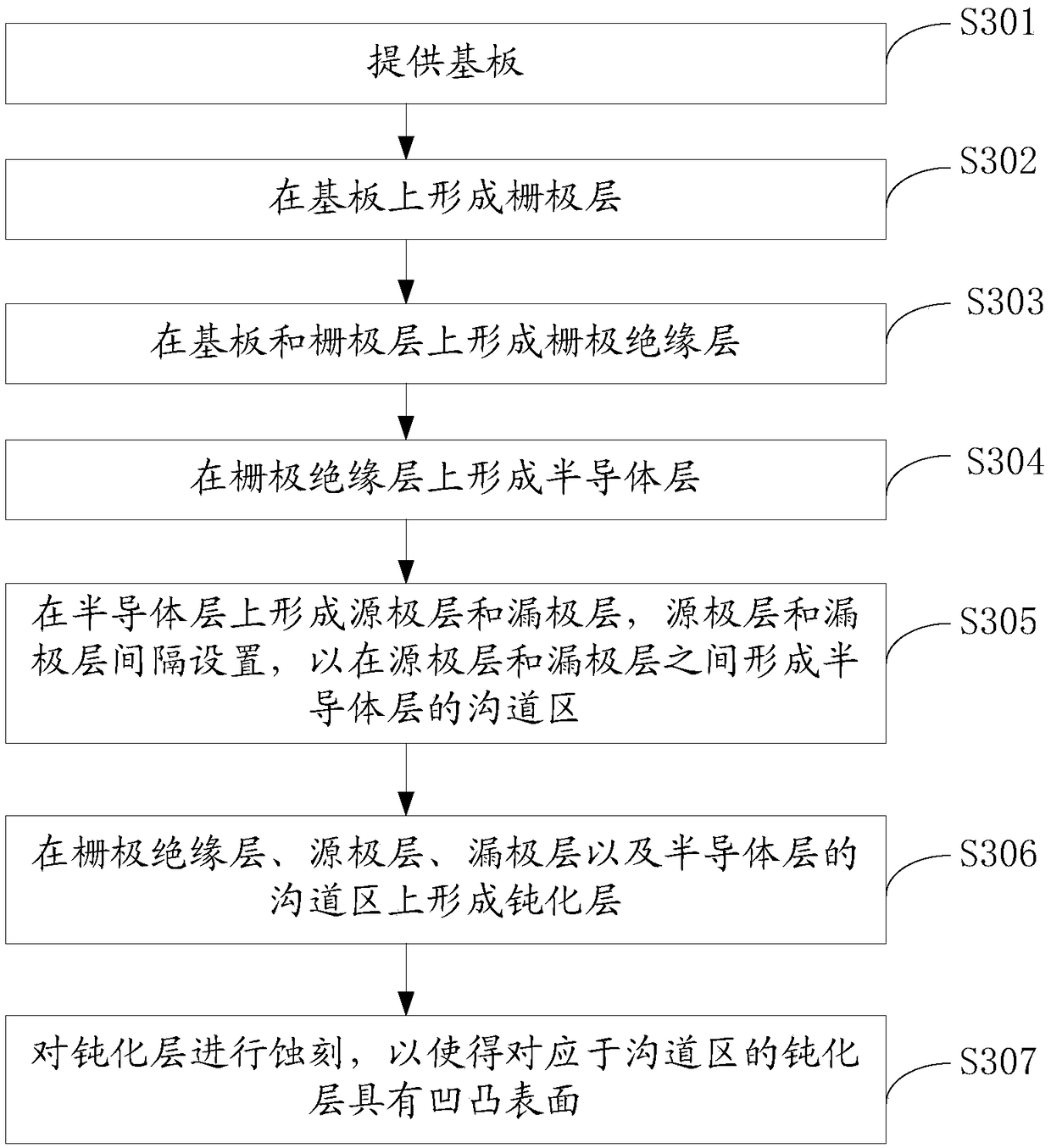
[0047] The technical solutions in the embodiments of the present application will be described clearly and completely in conjunction with the accompanying drawings in the embodiments of the present application. Obviously, the described embodiments are only a part of the embodiments of the present application, rather than all the embodiments. Based on the embodiments in this application, all other embodiments obtained by those skilled in the art without creative work fall within the protection scope of this application.

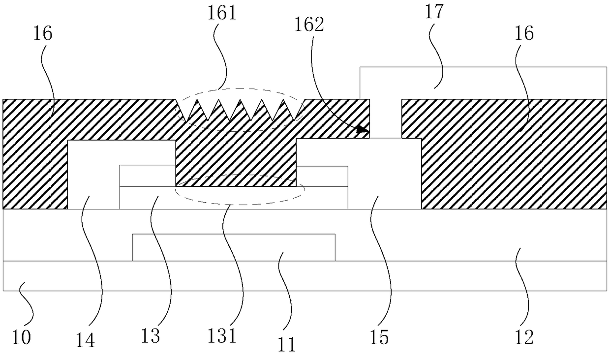
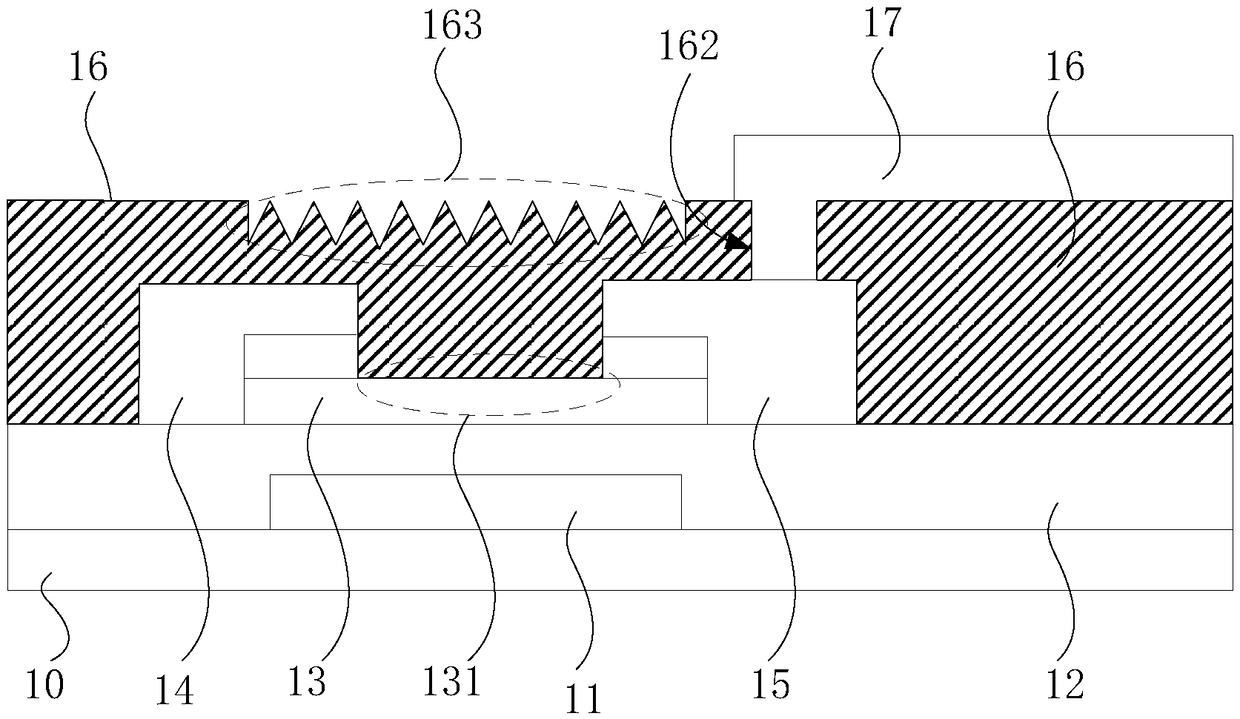
[0048] Refer to figure 1 In the thin film transistor provided by an embodiment of the present application, the thin film transistor includes a substrate 10, a gate layer 11, a gate insulating layer 12, a semiconductor layer 13, a source layer 14, a drain layer 15 and a passivation layer 16.

[0049] Among them, the substrate 10 may be, for example, a glass substrate or a substrate of other materials. The gate layer 11 serves as the gate of the thin film transistor ...


PUM


Abstract

The embodiment of the present application discloses a thin film transistor and a method of manufacturing the same. In the thin film transistor, a gate layer, a gate insulating layer, a semiconductor layer, a source layer, a drain layer, and a passivation layer are sequentially formed on a substrate; the passivation layer is formed on the gate insulating layer, the source layer, the drain layer, and the semiconductor layer of a channel region, wherein the passivation layer corresponding to the channel region has a concave-convex surface, and in the above manner, the aperture ratio can be ensured, the light that is irradiated onto the channel region of the semiconductor layer of the thin film transistor can be reduced, which is advantageous for improving the stability of the thin film transistor.

Description

Technical field [0001] This application relates to the technical field of thin film transistors, in particular to a thin film transistor and a manufacturing method thereof. Background technique [0002] Thin Film Transistor (TFT, Thin Film Transistor) as a switching device is widely used in display panels, such as liquid crystal display panels, OLED display panels, etc., and its electrical stability is one of the key factors affecting the performance of the display panel. [0003] The semiconductor channel layer is a structural component of the TFT. It is easy to form electron-hole pairs after being exposed to light, thereby forming a current, which will adversely affect the electrical characteristics of the TFT and reduce the stability of the TFT. In the working environment of TFT, such as when applied to a liquid crystal display panel, the TFT will be irradiated by backlight and external light, which will have a certain impact on the electrical characteristics of the TFT. The pri...

Claims


Application Information

Patent Timeline
IPC IPC(8): H01L29/786H01L21/336
CPCH01L29/66765H01L29/78633H01L29/78669
Inventor 孟小龙张瑞军
Owner TCL CHINA STAR OPTOELECTRONICS TECH CO LTD
Why Eureka
Try Eureka