Pixel array

A pixel array and pixel technology, applied in the field of pixel array, can solve problems such as inability to manufacture, and achieve the effect of reducing difficulty and reducing difficulty of production

Active Publication Date: 2018-05-01
EVERDISPLAY OPTRONICS (SHANGHAI) CO LTD
View PDF4 Cites 3 Cited by
  • Summary
  • Abstract
  • Description
  • Claims
  • Application Information

AI Technical Summary

Problems solved by technology

[0005] The present invention provides a pixel array, which is used to solve the problem that when the resolution of OLED in the prior art reaches more ...

Method used


Image

  • Pixel array
  • Pixel array
  • Pixel array

Examples


Embodiment 1

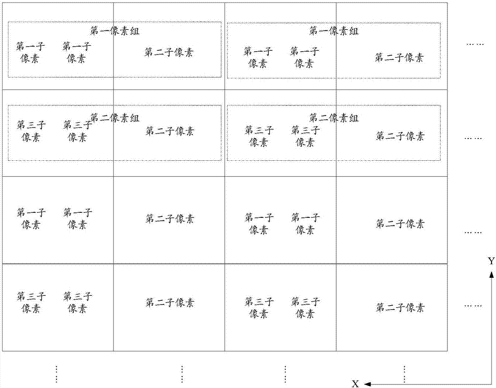
[0077] In the embodiment of the present invention, such as Figure 12 As shown, the first sub-pixel is R, the second pixel is B, the third sub-pixel is G, the first pixel group is R-R-B, and the second pixel group is G-G-B, then the first pixel group is continuously and repeatedly arranged along the first direction , the second pixel group is continuously and repeatedly arranged along the first direction, and, in the embodiment of the present invention, the first direction is a direction with an included angle of 45 degrees with the Y axis;

[0078]In the pixel array area, each minimum arrangement unit includes two different types of sub-pixels, and in the pixel array area, the B color is arranged in a second direction, that is, the second direction is parallel to the Y-axis direction;

[0079] In the pixel array area, the distances between R, G, and B in the first pixel group and the second pixel are equal;

[0080] The shape of the three sub-pixels R, G, and B is a rectangl...

Embodiment 2

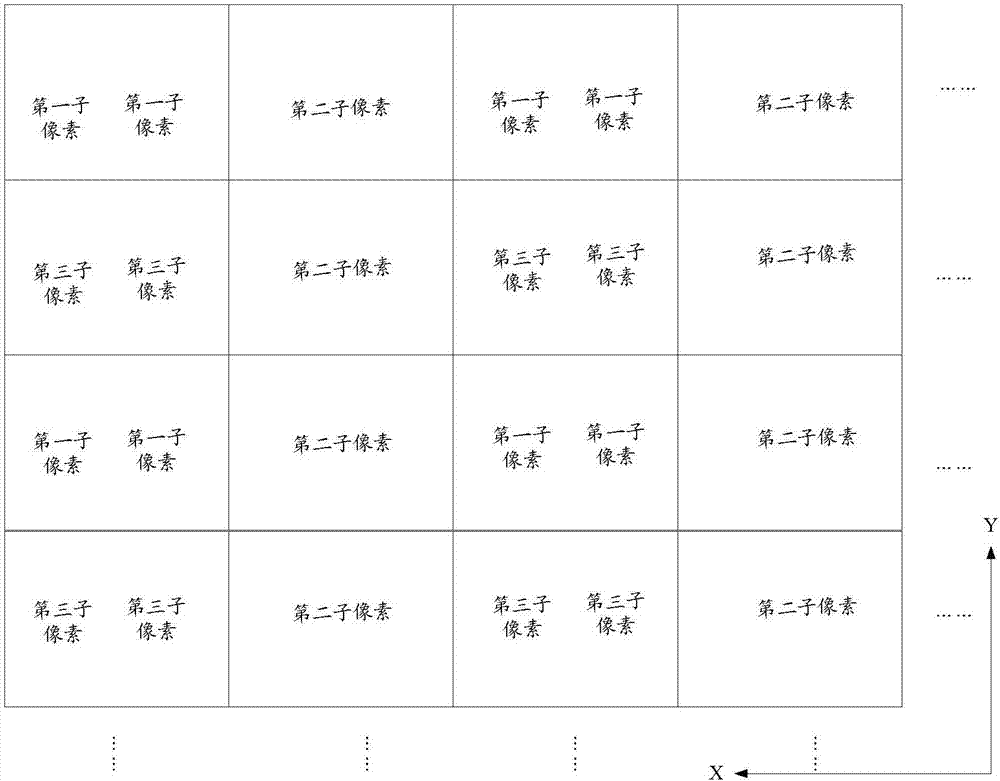
[0086] In order to better meet the high PPI requirement of OLED, in the embodiment of the present invention, as Figure 13 As shown, three sub-pixels are arranged in each minimum arrangement unit to improve the physical PPI of OLED;

[0087] Among them, the first sub-pixel is R, the second sub-pixel is B, the third sub-pixel is G, the first pixel group is R-R-B, and the second pixel group is G-G-B, then the first pixel group is continuously and repeatedly arranged along the first direction , the second pixel group is continuously and repeatedly arranged along the first direction;

[0088] In each smallest arrangement unit, B is located at the first intersection point of the smallest arrangement unit, R is located at any position on the line connecting the first intersection point of the smallest arrangement unit and the first vertex of the smallest arrangement unit, and B is located at the first intersection of the smallest arrangement unit Any position on the line between an...


PUM


Abstract

The invention provides a pixel array, which relates to the technical field of organic light-emitting diodes. The pixel array comprises a first pixel set and a second pixel set. The first pixel set comprises at least two first sub-pixels and a second sub-pixel, which are continuously arranged. The second pixel set comprises at least two third sub-pixels and a second sub-pixel, which are continuously arranged. The first pixel set and the second pixel set are repetitively arranged along the first direction. The straight line where the first pixel set lies and the straight line where the second pixel set lines are parallel to each other, and are alternatively and repetitively arranged. The first sub-pixel, the second sub-pixel and the third sub-pixel included in the at most four smallest arranging units of the pixel array are of the same in quantity. The invention is advantageous in that through the above pixel array, the problem of the prior art that openings corresponding to R color andG color are hard to be produced when OLED has high PPI can be effectively resolved; the luminance of three pixels can be guaranteed.

Description

technical field [0001] The invention relates to the technical field of light emitting diode display, in particular to a pixel array. Background technique [0002] In flat panel display technology, Organic Light-Emitting Diode (OLED) displays are famous for their thinness, active light emission, fast response speed, wide viewing angle, rich colors and high brightness, low power consumption, and high and low temperature resistance. It is recognized by the industry as the third generation of display technology after liquid crystal display (LCD). According to the driving method, OLED is divided into passive OLED (Passive Matrix OLED, PMOLED) and active OLED (Active Matrix OLED, AMOLED). PMOLED is also called passive matrix OLED, and AMOLED is also called active matrix OLED. PMOLED can only To produce small-sized, low-resolution display panels, AMOLED can realize large-sized, high-resolution panels because it integrates a thin-film transistor (TFT) and a capacitor in each pixel ...

Claims


Application Information

Patent Timeline
IPC IPC(8): H01L27/32
CPCH10K59/353H10K59/35
Inventor 陈凯凯高志豪屈晓娟
Owner EVERDISPLAY OPTRONICS (SHANGHAI) CO LTD
Why Eureka
Try Eureka