Charge pump circuit and memory

A charge pump and circuit technology, applied in the field of circuits, can solve the problems of large output terminal capacitance and large output voltage deviation, and achieve the effect of saving area, reducing output voltage ripple, and reducing output terminal capacitance

CN109428481AInactive Publication Date: 2019-03-05HEFEI GEYI INTEGRATED CIRCUIT CO LTD +1
0 Cites 5 Cited by

Patent Information

Authority / Receiving Office
CN · China
Patent Type
Applications(China)
Current Assignee / Owner
Publication Date
2019-03-05
Estimated Expiration
Not applicable · inactive patent

Smart Images

  • Figure 1
    Figure 1
  • Figure 2
    Figure 2
  • Figure 3
    Figure 3
Patent Text Reader

Abstract

Embodiments of the invention provide a charge pump circuit and a memory. The charge pump circuit comprises a charge pump and a comparator, and the charge pump circuit further comprises a ripple suppression circuit, wherein the ripple suppression circuit comprises an operational amplifier and a discharge module, a non-inverting input end of the operational amplifier is connected with a non-inverting input end of the comparator, an inverting input end of the operational amplifier is connected with a reference input voltage providing end of the comparator, a gain of the operational amplifier is greater than a gain of the comparator, the discharge module is connected with an output end of the operational amplifier and an output end of a charge pump, and when a voltage difference between a voltage of the non-inverting input end of the comparator and a reference input voltage is greater than or equal to voltage accuracy of the operational amplifier, the discharge module discharges the chargepump according to an output voltage of the operational amplifier. Through adoption of the charge pump circuit, output ripples of the charge pump circuit are reduced effectively, filter capacitance isreduced, and correspondingly, the area of the memory is reduced.
Need to check novelty before this filing date? Find Prior Art

Description

Technical field

[0001] The present invention relates to the field of circuit technology, in particular to a charge pump circuit and a memory. Background technique

[0002] In FLASH (flash memory), the charge pump circuit is used to generate high voltage, and the smaller the ripple of the charge pump output voltage in the charge pump circuit, the better. The size of the ripple is not only related to the charge pump's own ability to provide charge, but also related to the detection circuit of the charge pump circuit. The more accurate the detection circuit is and the faster the response, the smaller the ripple.

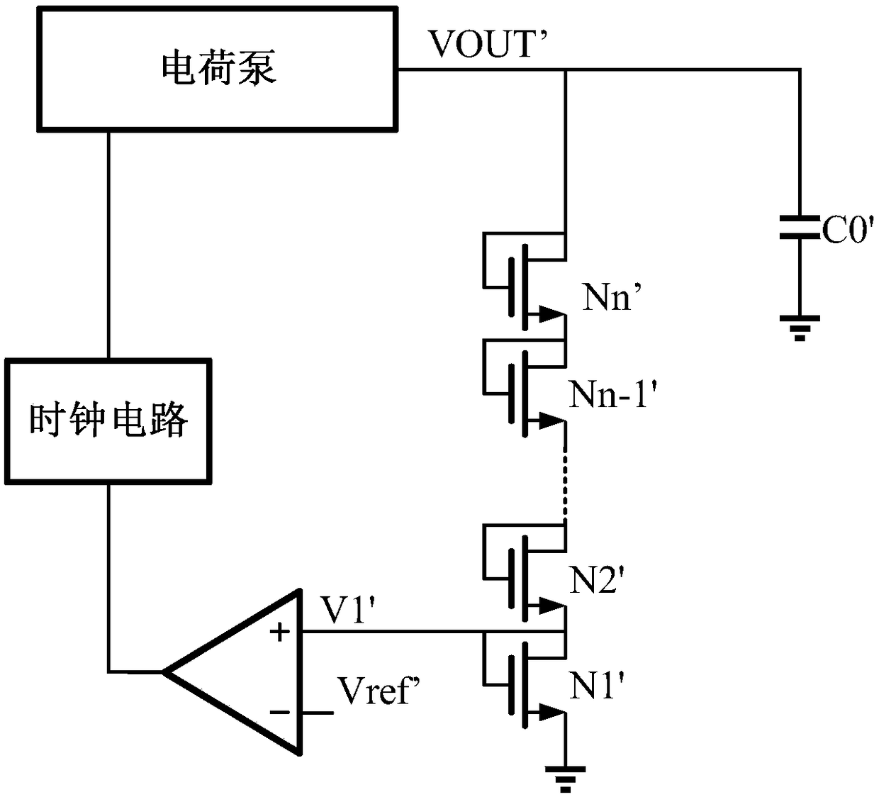
[0003] Such as figure 1 As shown, the detection circuit of the charge pump circuit in the prior art is realized by a detection string circuit, and the detection string circuit is composed of n NMOS (N1',..., Nn-1', Nn') connected in series in a diode manner . The comparator compares the voltage of the node V1' in the detection string with the reference voltage Vref'. The ...

Examples

Embodiment Construction

[0028] In order to make the above objectives, features and advantages of the present invention more obvious and understandable, the present invention will be further described in detail below with reference to the accompanying drawings and specific embodiments.

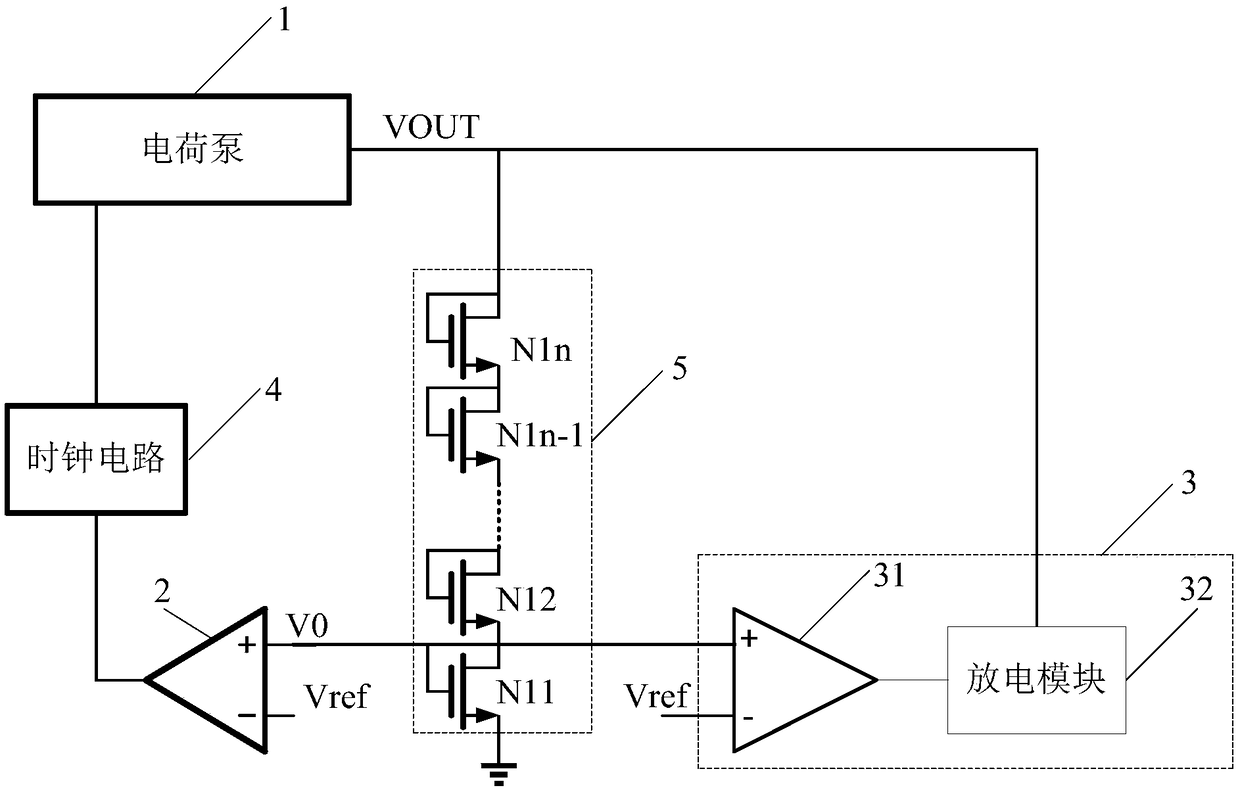
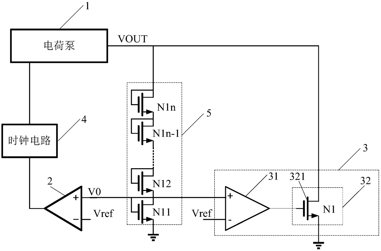
[0029] Reference figure 2 , Which shows a structural block diagram of an embodiment of a charge pump circuit of the present invention, the charge pump circuit includes a charge pump 1 and a comparator 2, the charge pump circuit also includes a ripple suppression circuit 3, the ripple suppression circuit 3 includes : Operational amplifier 31, the non-inverting input terminal of operational amplifier 31 is connected to the non-inverting input terminal of comparator 2, and the inverting input terminal of operational amplifier 31 is connected to the supply terminal of the reference input voltage Vref of comparator 2; the gain of operational amplifier 31 is greater than The gain of the comparator 2; the discharge module 32, t...