Circuit board and manufacturing method thereof
A circuit board manufacturing and circuit board technology, applied in the directions of printed circuits, printed circuits, printed circuit components, etc., can solve the problems of corrosion of the nickel layer, peeling off of the gold layer, corrosion of the nickel layer, etc., to reduce the contact area, prevent The effect of peeling off and delaying the reaction time
- Summary
- Abstract
- Description
- Claims
- Application Information
AI Technical Summary
Problems solved by technology
Method used
Image
Examples
no. 1 example
[0050] Taking the manufacture of a single-layer circuit board as an example below, the method for manufacturing the circuit board 100 provided by the technical solution will be described. The method for manufacturing the circuit board 100 includes the following steps:
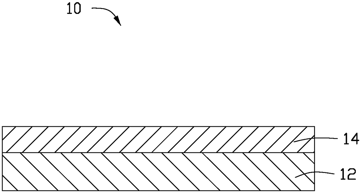
[0051] For step S1, see figure 1 , providing a copper-clad substrate 10, the copper-clad substrate 10 is a single-sided copper-clad substrate. The copper-clad substrate 10 may be a flexible copper-clad substrate or a rigid copper-clad substrate. The copper-clad substrate 10 includes an insulating layer 12 and a copper foil layer 14 formed on the surface of the insulating layer 12, and the thickness of the copper foil layer 14 may be 2um.
[0052] In other embodiments, the copper-clad substrate 10 may also be a double-layer copper-clad substrate.
[0053] In the second step S2, please refer to Figure 2-6 , forming the copper foil layer 14 into a conductive structure. The conductive structure 14 includes a p...
no. 2 example
[0071] see Figure 9 The circuit board 200 provided by the second embodiment is basically the same as the circuit board 100 provided by the first embodiment, the difference is that the cross-sectional shape of the protruding edge 244 of the circuit board 200 is a rectangle, and the protruding edge 244 The height is less than the height of the quadrilateral 142 .
[0072] It can be understood that the conductive structure 14 of the circuit board 200 can be formed by two etching processes.
no. 3 example
[0074] see Figure 10 The circuit board 300 provided by the third embodiment is basically the same as the circuit board 100 provided by the first embodiment, except that the cross-sectional shape of the protruding edge 344 of the circuit board 300 is trapezoidal, and the height of the protruding edge 344 is less than the height of the quadrilateral 142 .
[0075] It can be understood that the conductive structure 14 of the circuit board 300 can be formed by two etching processes.
PUM
 Abstract
Description
Claims
Application Information


