Array substrate and manufacturing method, and liquid crystal display panel

A technology of an array substrate and a manufacturing method, which is applied in the field of liquid crystal display, can solve the problems of increasing the risk of light leakage and increasing the cost of materials, and achieve the effects of improving the yield rate of the process, improving the flexibility of the process, and not being easy to etch

Active Publication Date: 2021-09-21
KUSN INFOVISION OPTOELECTRONICS
View PDF15 Cites 0 Cited by
  • Summary
  • Abstract
  • Description
  • Claims
  • Application Information

AI Technical Summary

Problems solved by technology

[0007] However, increasing the aperture ratio of pixels in design will increase the risk of light leakage; using polarizers with APCF function in materials will increase material costs

Method used


Image

  • Array substrate and manufacturing method, and liquid crystal display panel
  • Array substrate and manufacturing method, and liquid crystal display panel
  • Array substrate and manufacturing method, and liquid crystal display panel

Examples


Embodiment Construction

[0071] The present invention will be described in further detail below in conjunction with the accompanying drawings and specific embodiments, but the implementation scope of the present invention is not limited thereto.

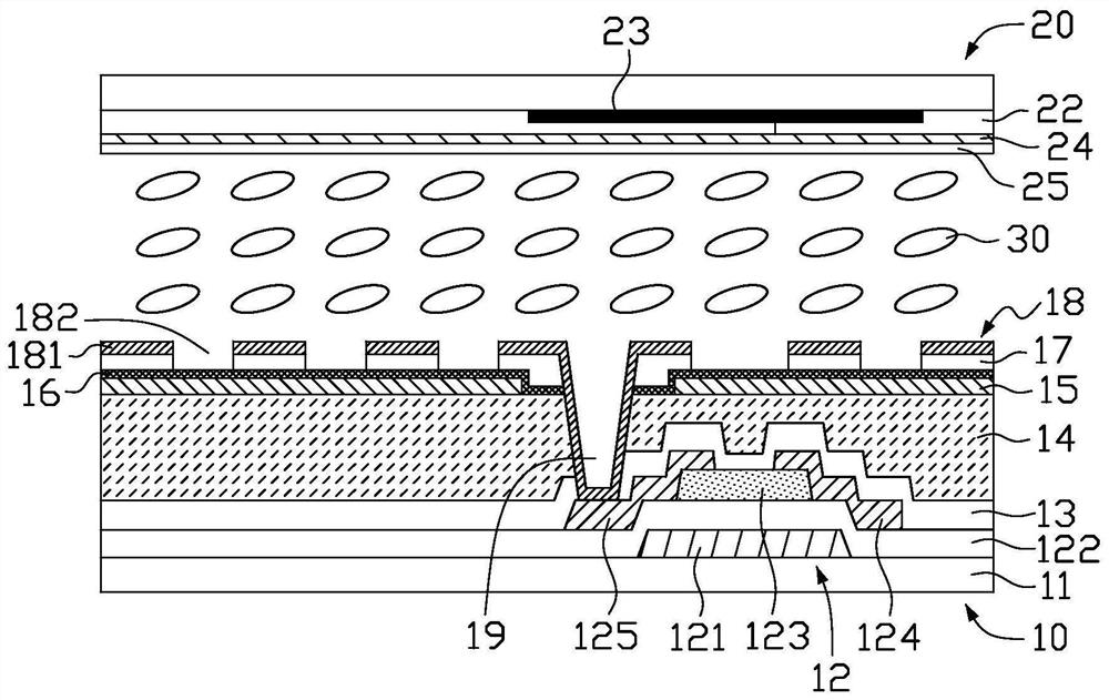
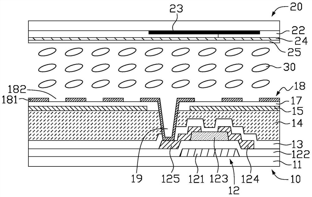
[0072] Please refer to figure 1 An embodiment of the present invention provides a liquid crystal display panel, including an array substrate 10 , a color filter substrate 20 disposed opposite to the array substrate 10 , and a liquid crystal layer 30 disposed between the array substrate 10 and the color filter substrate 20 .

[0073] Specifically, the array substrate 10 includes:

[0074] Substrate 11;

[0075] A TFT array formed on the substrate 11, the TFT array includes a plurality of TFTs 12 arranged in an array;

[0076] A first insulating layer 13 covering the TFT array;

[0077] a flat layer 14 covering the first insulating layer 13;

[0078] a common electrode 15 formed on the planar layer 14;

[0079] a second insulating layer 16 covering the co...


PUM


Abstract

An array substrate, a manufacturing method, and a liquid crystal display panel, wherein the array substrate includes: a substrate; a TFT array formed on the substrate, the TFT array includes a plurality of TFTs arranged in an array; a first insulating layer covering the TFT array; a flat layer covering the first insulating layer; a common electrode formed on the flat layer; a second insulating layer covering the common electrode; a third insulating layer covering the second insulating layer; a plurality of pixel electrodes formed on the third insulating layer , each pixel electrode is connected to a conductive electrode of the corresponding TFT through a contact hole, each pixel electrode has a comb-like structure with electrode strips and slits, and the third insulating layer is on the electrode strip corresponding to each pixel electrode The remaining area outside the position is etched away to expose the second insulating layer below, wherein the third insulating layer and the second insulating layer are made of different materials, and the etching selectivity ratio between the third insulating layer and the second insulating layer is greater than 1. The film thickness of the second insulating layer is smaller than the film thickness of the third insulating layer.

Description

technical field [0001] The invention relates to the technical field of liquid crystal display, in particular to an array substrate, a manufacturing method and a liquid crystal display panel. Background technique [0002] With the development of display technology, liquid crystal display panels (Liquid Crystal Display, LCD) are more and more popular due to their advantages of lightness and low radiation. The liquid crystal display panel includes a color filter substrate (color filter, CF) and an array substrate (TFT array substrate) opposite to each other, and a liquid crystal layer (LC layer) sandwiched between them. [0003] When the liquid crystal display panel is working, by applying the driving voltage and the common voltage to the pixel electrode and the common electrode respectively to generate an electric field between the liquid crystal layer, the deflection direction of the liquid crystal molecules will change with the difference between the applied driving voltage ...

Claims


Application Information

Patent Timeline
Patent Type & Authority Patents(China)
IPC IPC(8): G02F1/1362G02F1/1343H01L27/12H01L21/77
CPCG02F1/134309G02F1/136213G02F1/136227G02F1/136295H01L27/1248H01L27/1259
Inventor 钟德镇郑会龙沈家军姜丽梅
Owner KUSN INFOVISION OPTOELECTRONICS
Why Eureka
Try Eureka