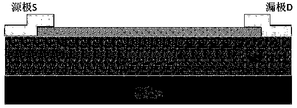
Display device

A display device and display panel technology, applied in static indicators, instruments, etc., can solve problems such as poor picture, and achieve the effect of reducing extra power consumption and saving circuit space

Active Publication Date: 2019-03-08
NANJING CEC PANDA LCD TECH
View PDF6 Cites 12 Cited by
  • Summary
  • Abstract
  • Description
  • Claims
  • Application Information

AI Technical Summary

Problems solved by technology

[0008] In order to solve the above technical problems, the present invention provides a display device, which can solve the problem of poor picture caused by the demultiplexing circuit in the display device, save circuit space, and reduce the extra power consumption caused by compensation

Method used


Image

  • Display device
  • Display device
  • Display device

Examples


Embodiment 1

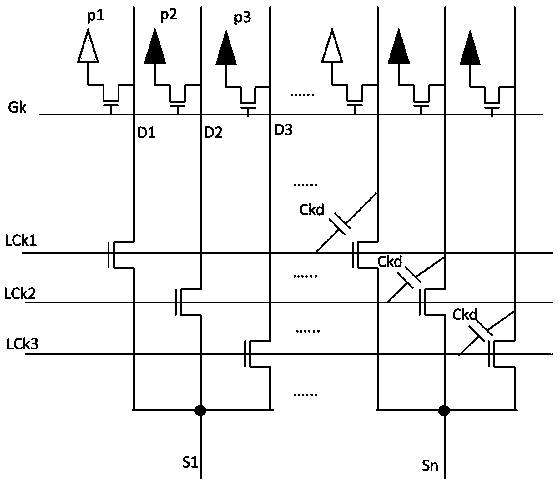
[0059] Figure 8 It is a schematic diagram of a partial structure of a display device in an embodiment of the present invention. The Mux ratio of the demultiplexing circuit in this embodiment is 1:3.

[0060] Taking the switch group connected to the first data line S1 and the corresponding multiple second data lines D1, D2, D3 as an example, the switch group includes 3 strobe switches M1, M2, M3, 3 strobe switches M1, The first channel ends of M2 and M3 are connected to each other and connected to the first data line S1, and the second channel ends of the gating switches M1, M2, M3 are respectively connected to three second data lines D1, D1, and D1 in the same second data line group. D2, D3, the control ends of the gating switches M1, M2, M3 are respectively connected to the switch control lines LCK1, LCK2, LCK3, and the gating parasitic capacitance Ckd1 is generated between the control ends of the gating switches M1, M2, M3 and the second channel end respectively , Ckd2, Ck...

Embodiment 2

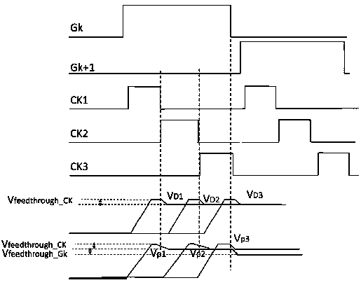
[0068] The difference between the second embodiment and the first embodiment is that the falling edge of the last switch signal (ie, the switch signal CK3 ) is no later than the falling edge of the high-level phase of the scanning signal Gk.

[0069] In Embodiment 2, the waveforms of scanning signals Gk, Gk+1, switch control signals CK1, CK2, CK3 and compensation signals CK1', CK2' are as follows Figure 13 shown. Since the closing of the gate switch M3 will not only affect the potential V of the second data line D3 D 3, it will also affect the pixel voltage Vp3. When the last strobe switch is closed, the falling edges of the compensation signals CK1' and CK2' occur at the same time, and the compensation signals CK1' and CK2' cause the pixel voltage Vp1 and Vp2 The generated compensation voltage difference and the gate feed-through voltage (V feedthrough_CK ) is consistent in magnitude and positive or negative, the compensation voltage difference and the gate feed-through vo...


PUM


Abstract

The invention discloses a multi-purpose demultiplexing circuit and a display device, and belongs to the field of display technology. The multi-path demultiplexing circuit comprises: n first data lines, n switch groups respectively connected with the n first data lines, a switch driving circuit, m switch control lines connected to the switch driving circuit, a compensation drive circuit and m-1 compensation lines connected to the compensation drive circuit, wherein n and m are an integer greater than 1. The m-1 compensation lines respectively compensate gated feed-through voltage caused by theclosing of m-1 non-last gating switches; and gated feed-through voltage caused by the closing of the last gating switch is not compensated or compensated by being regulated along with compensating voltage difference caused by m-1 compensation signals with common voltage according to situations. Only by additionally arranging m-1 compensation lines, the effect of uniformity of feed-through voltagereceived by each column of pixels can be achieved. Thereby, the problem of poor display caused by the closing of the gating switches can be solved; and circuit space can be saved, and additional powerconsumption brought by the compensation is lowered.

Description

technical field [0001] The invention belongs to the field of display technology, and in particular relates to a display device. Background technique [0002] The demultiplexing circuit (Demux technology) is widely used in display devices. It can convert the data voltage output by the data drive circuit (SourceIC) to 1:m (such as 1:2, 1:3, etc., m is an integer greater than 1, 1: m is the Mux ratio) in the form of time-sharing transmission to the corresponding m second data lines, the number of the first data lines connected to the data driving circuit can be reduced by at least half compared to the number of the second data lines connected to the pixel unit, and can Reduce the number of ICs, thereby reducing panel design costs and saving layout space, reducing the lower frame of the panel, so that the panel can meet the requirements of a narrower frame. [0003] Due to the adoption of the Demux technology, multiple thin film transistors (TFTs) need to be used as gating swit...

Claims


Application Information

Patent Timeline
Patent Type & Authority Applications(China)
IPC IPC(8): G09G3/20
CPCG09G3/20G09G2330/021
Inventor 文超平黄威徐竹青
Owner NANJING CEC PANDA LCD TECH
Why Eureka
Try Eureka