Display substrate, manufacturing method thereof and display device

A technology for display substrates and substrate substrates, which is applied in the manufacture of semiconductor/solid-state devices, electrical components, and electrical solid-state devices, etc., can solve the problems of low packaging reliability of flexible display devices, suppress the intrusion of water and oxygen, and improve the reliability of packaging. sexual effect

Inactive Publication Date: 2019-03-08
BOE TECH GRP CO LTD
View PDF9 Cites 13 Cited by
  • Summary
  • Abstract
  • Description
  • Claims
  • Application Information

AI Technical Summary

Problems solved by technology

[0005] Embodiments of the present invention provide a display substrate, a manufacturing method thereof, and a display device, which can solve the problem of low packaging reliability of flexible display devices in related technologies

Method used


Image

  • Display substrate, manufacturing method thereof and display device
  • Display substrate, manufacturing method thereof and display device
  • Display substrate, manufacturing method thereof and display device

Examples


Embodiment Construction

[0043] In order to make the objectives, technical solutions, and advantages of the present invention clearer, the embodiments of the present invention will be described in further detail below in conjunction with the accompanying drawings.

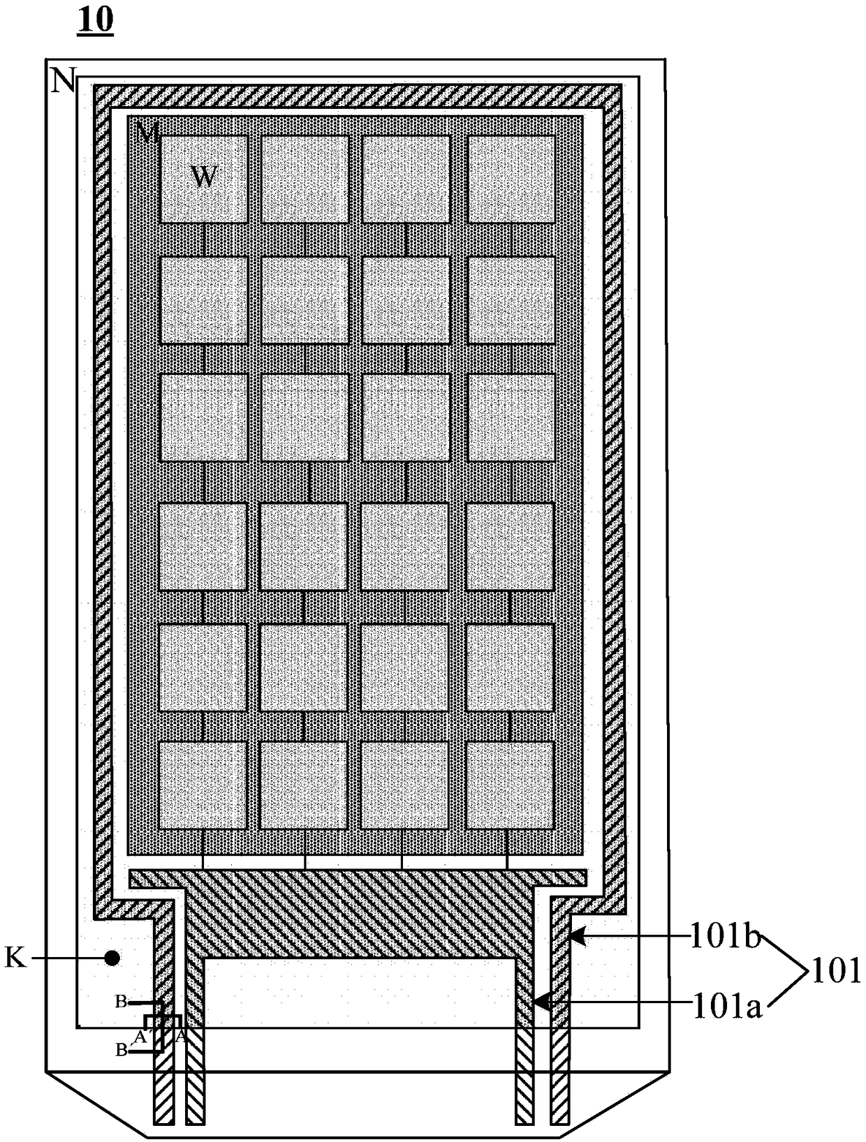
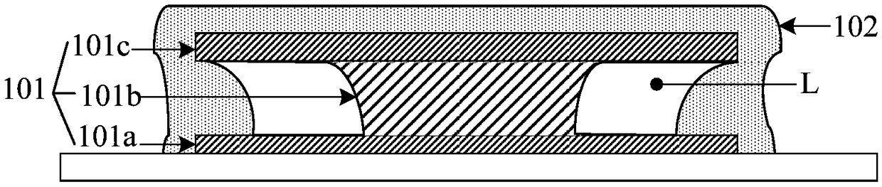
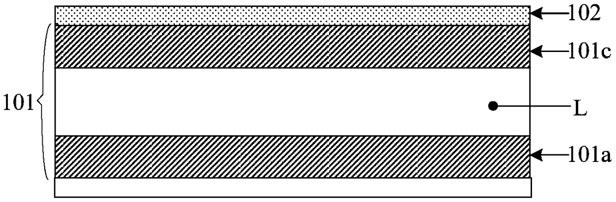
[0044] At present, the flexible display device includes: a base substrate, and a TFT, a light emitting device, and a thin-film encapsulation layer sequentially arranged on the base substrate. Among them, the TFT includes a gate pattern, a gate insulating layer, an active layer, and a source and drain pattern. The source and drain patterns include source and drain electrodes located in the display area and power signal lines located in the non-display area, that is, the power signal lines are prepared in the same layer as the source and drain electrodes. The light emitting device includes an anode, a light emitting layer, and a cathode stacked in a direction away from the base substrate.

[0045] figure 1 Shows a schematic top view of a flexibl...


PUM


Abstract

The invention discloses a display substrate, a manufacturing method thereof and a display device, and belongs to the technical field of displaying. The display substrate comprises a substrate, a thinfilm transistor, a light-emitting device and a package structure, wherein the thin film transistor, the light-emitting device and the package structure are sequentially arranged on the substrate, thethin film transistor comprises a gate pattern, a gate insulation layer, an active layer and a source-drain pattern, the source-drain pattern comprises a source, a drain and at least one power signal line, the source and the drain are arranged in the display region, the at least one power signal line is arranged in a non-display region, at least one side edge of each power signal is coated with anelectrode block, the light-emitting device comprises a first electrode, a light-emitting layer and a second electrode which are laminated along a direction far away from the substrate, and the electrode block and the first electrode are obtained by fabrication at the same layer. By coating the side edge of the power signal line arranged in the non-display region with the electrode block, the sideedge, coated with the electrode block, of the power signal line can be prevented from being drilled, and the package reliability of the display substrate is improved.

Description

Technical field [0001] The present invention relates to the field of display technology, in particular to a display substrate, a manufacturing method thereof, and a display device. Background technique [0002] At present, flexible display devices are usually packaged in a thin film packaging (ThinFilm Encapsulation, TFE) manner. The principle of thin film packaging is to use a dense thin film packaging layer to block water and oxygen, so that the metal cathode and luminescent materials inside the flexible display device are protected from water and oxygen. [0003] The flexible display device includes: a base substrate, and a thin film transistor (ThinFilm Transistor, TFT), a light emitting device, and a thin film packaging layer sequentially arranged on the base substrate. Among them, the TFT includes a gate pattern, a gate insulating layer, an active layer, and a source-drain pattern that are stacked. The source and drain patterns include source and drain electrodes located in...

Claims


Application Information

Patent Timeline
Patent Type & Authority Applications(China)
IPC IPC(8): H01L27/32H01L51/52
CPCH10K59/131H10K50/844H10K59/1201H01L27/124H10K71/00
Inventor 张子予张嵩周伟峰
Owner BOE TECH GRP CO LTD
Why Eureka
Try Eureka