
Method for judging high-density semiconductor chip pin deformation by multi-algorithm superposition

A semiconductor, high-density technology, used in computing, image data processing, instruments, etc., to reduce labor costs and time, and avoid cost increases

Inactive Publication Date: 2019-03-12
SHENZHEN KINGCOS AUTOMATION ROBOT EQUIP CO LTD
View PDF3 Cites 0 Cited by
  • Summary
  • Abstract
  • Description
  • Claims
  • Application Information

AI Technical Summary

Problems solved by technology

[0004] The purpose of the present invention is to solve the problem in the prior art that a technology that can detect bad chips is needed to reduce or prevent the outflow of bad chips, and proposes a method for judging pin deformation of high-density semiconductor chips by superposition of multiple algorithms

Method used


Image

  • Method for judging high-density semiconductor chip pin deformation by multi-algorithm superposition
  • Method for judging high-density semiconductor chip pin deformation by multi-algorithm superposition
  • Method for judging high-density semiconductor chip pin deformation by multi-algorithm superposition

Examples


Embodiment 1

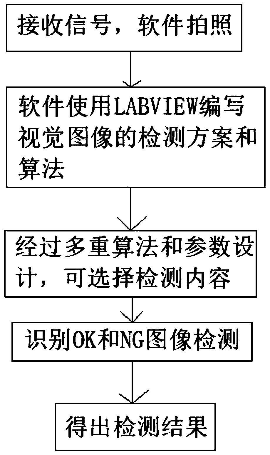
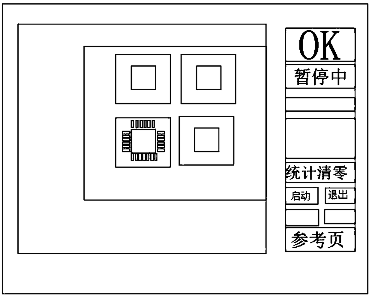
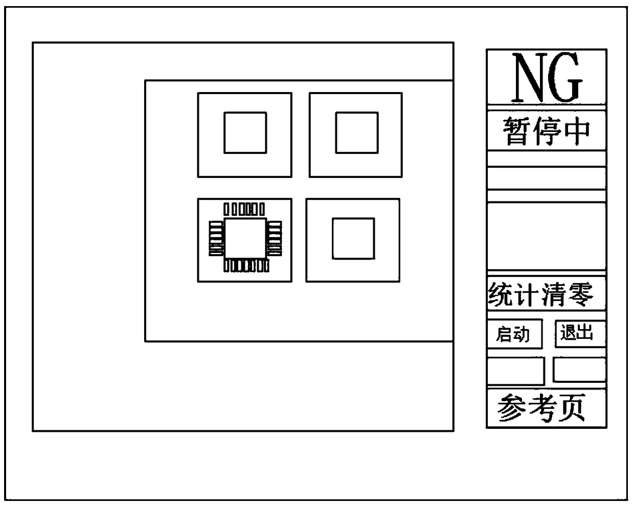
[0027] refer to Figure 1-3 , a multi-algorithm superposition method for judging pin deformation of a high-density semiconductor chip is characterized in that it includes PC-side hardware and software, and the PC-side hardware and software are responsible for detecting whether the chip pins are good or bad, and the detection steps are:

[0028] 1.1) After receiving the detection signal, the software triggers to take pictures;

[0029] 1.2) The software uses LABVIEW to write the detection scheme and algorithm of visual image;

[0030] 1.3) After multiple algorithms and parameter design, the number of pins is detected;

[0031] 1.4) After successful identification of OK and NG, the semiconductor chip can be detected by combining detection options according to requirements;

[0032] 1.5) Combine all test results to get the final result.

[0033] After the image is binarized by software, the pins of the chip are processed by algorithm, the results are obtained according to the ...

Embodiment 2

[0040] refer to Figure 1-3 , a multi-algorithm superposition method for judging pin deformation of a high-density semiconductor chip, characterized in that it includes PC-side hardware and software, and the PC-side hardware and software are responsible for detecting whether the chip pins are good or bad, and the detection steps are:

[0041] 1.1) The PC-side hardware uses a visual board to support the software;

[0042] 1.2) In terms of software, LABVIEW is used to write the detection scheme and algorithm of visual image, which is used to detect the discrimination result;

[0043] 1.3) After receiving the detection signal, the software triggers to take pictures;

[0044] 1.4) After multiple algorithms and parameter design, detect image matching;

[0045] 1.5) After successful identification of OK and NG, the semiconductor chip can be tested according to the combination of detection options according to the requirements;

[0046] 1.6) Combine all test results to get the fin...

Embodiment 3

[0054] refer to Figure 1-3 , a multi-algorithm superposition method for judging the pin deformation of a high-density semiconductor chip, characterized in that it includes PC-side hardware and software, and the PC-side hardware and software are responsible for detecting whether the chip pins are good or bad, and the detection steps are:

[0055] 1.1) The PC-side hardware uses a visual board to support the software;

[0056] 1.2) In terms of software, LABVIEW is used to write the detection scheme and algorithm of visual image, which is used to detect the discrimination result;

[0057] 1.3) After receiving the detection signal, the software triggers to take pictures;

[0058] 1.4) After multiple algorithms and parameter design, the length deviation between terminals is detected;

[0059] 1.5) After successful identification of OK and NG, the semiconductor chip can be tested according to the combination of detection options according to the requirements;

[0060] 1.6) Combin...


PUM


Abstract

The invention discloses a method for judging high-density semiconductor chip pin deformation by multi-algorithm superposition. The method adopts PC (personal computer) terminal hardware and software,and the PC terminal hardware and software is used for detecting whether a chip pin is good or not. A detecting method includes the steps: enabling the PC terminal hardware to adopt a visual interfacecard to support the software; enabling the software to compile a detecting scheme and an algorithm of a visual pattern by an LABVIEW and to be used for detecting judging results; triggering picture taking by the software after detecting signals are received; detecting the number of the pin through multiple algorithms and parameter design; combining detection options according to requirements by successful identification of OK and NG to detect a semiconductor chip, acquiring a final result. According to the method, the PC terminal hardware and software is used for detecting whether the chip pinis good or not, the detecting scheme and the algorithm of the visual pattern are compiled by the LABVIEW, so that judging results are detected, an NG result graph can display defective number of thepin, defective image matching and defective terminal deviation, and the method can effectively control defective chips to flow into a market or to be produced.

Description

technical field [0001] The invention relates to the technical field of appearance detection of semiconductor chip pins, in particular to a method for judging deformation of high-density semiconductor chip pins by superposition of multiple algorithms. Background technique [0002] In modern industrial automation, the application of chips is becoming more and more extensive, and the types and structures of chips are becoming more and more complex and precise. If the feet are deformed or the appearance is damaged, these bad chips will flow into the equipment and use, which will bring more cost and time for rework. [0003] At present, in the existing technology, it is impossible to effectively control the flow of bad chips into the market or production, so the cost caused by bad chip pins or appearance is increased, and labor costs and time are also increased. Contents of the invention [0004] The purpose of the present invention is to solve the problem in the prior art tha...

Claims


Application Information

Patent Timeline
IPC IPC(8): G01N21/88G06T7/00
CPCG01N21/8851G01N2021/8887G06T7/0004
Inventor 康远潺姜胜林赵俊范旭阳周元辰
Owner SHENZHEN KINGCOS AUTOMATION ROBOT EQUIP CO LTD
Learn More