
A Reference Voltage Source Circuit Structure Suitable for Image Sensors

A reference voltage source, image sensor technology, applied in instruments, regulating electrical variables, control/regulating systems, etc., can solve problems such as large size, change, thermal noise, etc., to reduce small signal impedance, eliminate the influence of temperature coefficient, The effect of eliminating the bias circuit

Active Publication Date: 2020-07-28
CHENGDU LIGHT COLLECTOR TECH
View PDF10 Cites 0 Cited by
  • Summary
  • Abstract
  • Description
  • Claims
  • Application Information

AI Technical Summary

Problems solved by technology

However, in the output branch, on the one hand, the resistance value of the resistance will change with the temperature, and at the same time, a certain amount of thermal noise will be generated; Used as a PN junction, the device is generally larger in size, and is only used to provide a negative temperature characteristic voltage in the output branch

Method used


Image

  • A Reference Voltage Source Circuit Structure Suitable for Image Sensors
  • A Reference Voltage Source Circuit Structure Suitable for Image Sensors
  • A Reference Voltage Source Circuit Structure Suitable for Image Sensors

Examples


Embodiment Construction

[0054] The technical problem to be solved by the present invention is mainly to propose a reference voltage source circuit applied to a CIS chip under the double-well CMOS process, the purpose is to further improve the noise and PSRR characteristics of the internal reference voltage of the chip system, and reduce or eliminate as much as possible the noise in the imaging system. In the system, due to the noise introduced by the reference voltage current.

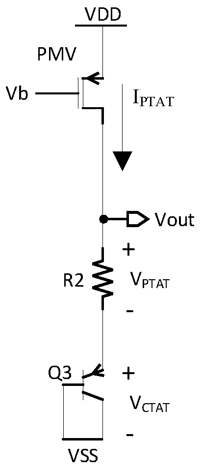
[0055] The invention is improved based on the structure of the conventional first-order bandgap reference voltage source. The general working principle of the conventional structure is to subtract the voltage difference between the positive and negative terminals of a resistor R1 from the voltage of the two PN junctions, thereby generating a PTAT current proportional to the temperature; and then mirroring the current to another output branch, where On the branch, the PTAT current flows through a resistor R2 to generate a PTAT...


PUM


Abstract

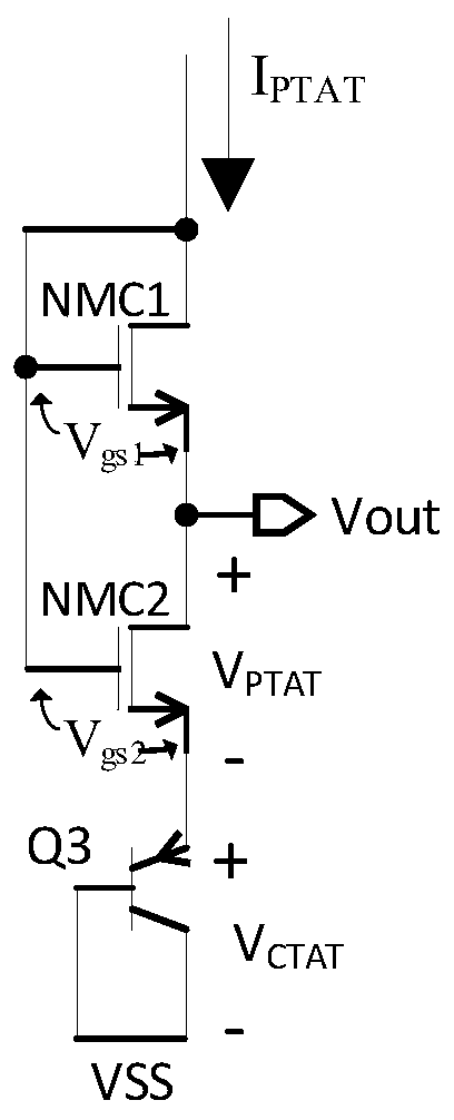
The invention discloses a reference voltage source circuit structure suitable for an image sensor. Based on the structure of a conventional first-order band-gap reference source of a double-well CMOSprocess, a current mirror is adopted to clamp nodes X and Y, a resistor for producing PTAT voltage in a conventional circuit is omitted and is replaced by an NMOS pipe column structure, meanwhile BJTof an output branch is omitted, one BJT for producing , PTAT current is reused, and accordingly the purpose of negative temperature voltage is achieved. The noise and PSRR characteristics of internalreference voltage of a chip system can be further improved, and noise introduced by reference voltage and current in an imaging system is reduced as much as possible or eliminated.

Description

technical field [0001] The invention relates to the technical field of image sensor design and application, and more particularly, relates to a circuit structure of a low-noise high-PSRR reference voltage source suitable for a CMOS image sensor. Background technique [0002] CMOS image sensor (CIS) chips have been continuously developed in recent years, and have gradually replaced CCDs and are widely used in various portable imaging electronic equipment, security monitoring equipment, and vehicle electronics. For the design purpose of high performance requirements and low power consumption and small size, noise and anti-interference in chips have become one of the most concerned issues for designers. [0003] Many circuit modules in the CIS chip system require corresponding reference voltages and bias currents to ensure stable and normal working conditions. Due to the actual use, there is a lot of noise in the external power supply, which cannot be directly applied to the s...

Claims


Application Information

Patent Timeline
Patent Type & Authority Patents(China)
IPC IPC(8): G05F1/56
CPCG05F1/56
Inventor 芮松鹏蔡化陈飞高菊
Owner CHENGDU LIGHT COLLECTOR TECH
Learn More