Optical network for a hybrid main memory of a dynamic random access memory and a nonvolatile memory

A dynamic random, non-volatile technology, applied in static memory, electromagnetic network arrangement, instruments, etc., can solve the problem of inability to support multi-level mixed main memory system, high communication delay of combined main memory architecture, and poor parallelism of main memory architecture and other issues to achieve the effect of improving scalability, achieving effective support, and improving parallelism

Active Publication Date: 2019-03-26
XIDIAN UNIV
View PDF9 Cites 0 Cited by
  • Summary
  • Abstract
  • Description
  • Claims
  • Application Information

AI Technical Summary

Problems solved by technology

Due to the long-distance electrical interconnection between the storage controller and the dynamic random access memory DRAM and the phase change random access memory PRAM, it will lead to high communication delay and low energy efficiency of the combined main memory architecture. The bus-type interconnection between them leads to the problem of poor parallelism of the main memory architecture. In addition, because it adopts the same-level distribution of DRAM and PRAM, there is no interconnection between the two types of memory, so it can only support same-level Main memory architecture system, but cannot support multi-level mixed main memory system

Method used


Image

  • Optical network for a hybrid main memory of a dynamic random access memory and a nonvolatile memory
  • Optical network for a hybrid main memory of a dynamic random access memory and a nonvolatile memory
  • Optical network for a hybrid main memory of a dynamic random access memory and a nonvolatile memory

Examples


Embodiment Construction

[0030] The present invention will be further described in detail below in conjunction with the accompanying drawings and specific embodiments.

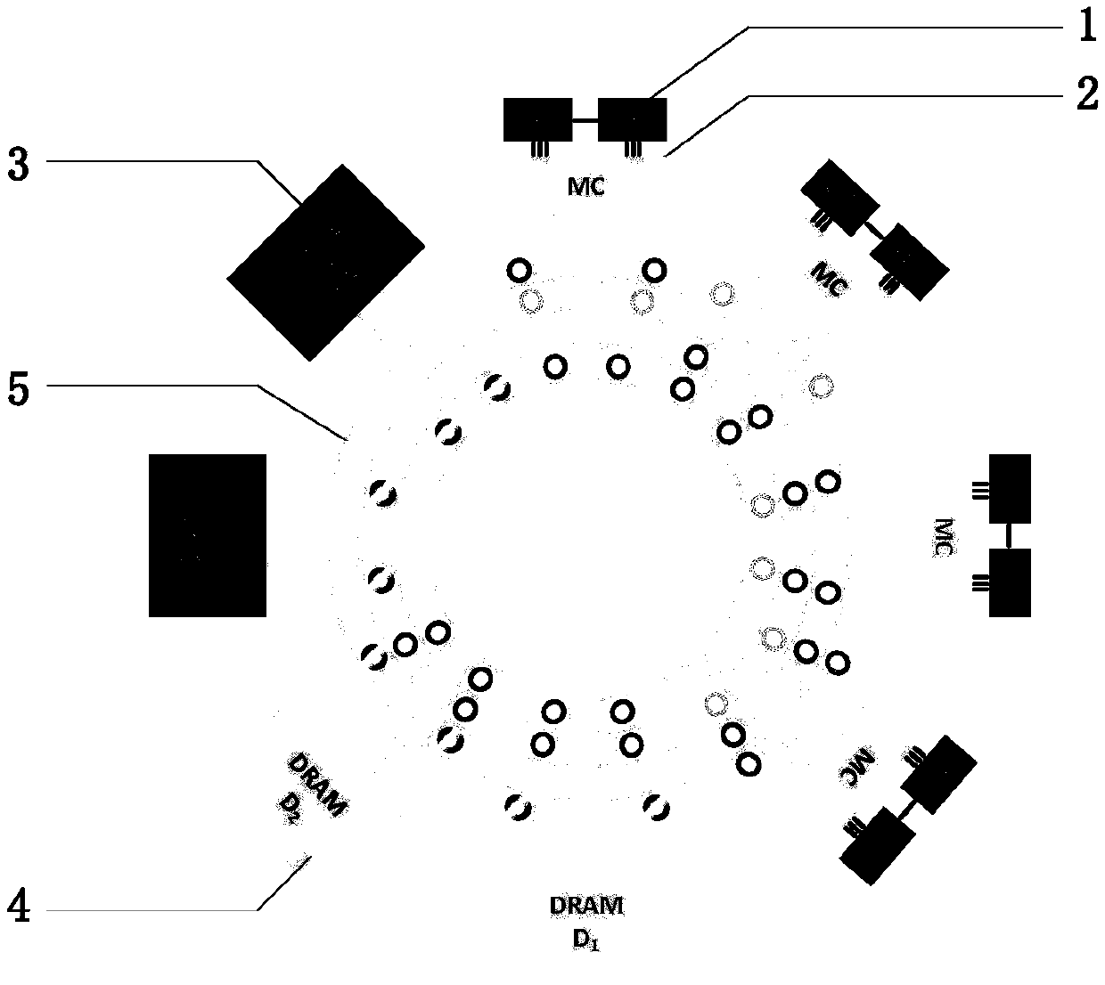
[0031] The optical network of the present invention includes: n computing nodes 1, i memory controller modules 2, k dynamic random access memory DRAM modules 3, m nonvolatile memory NVM modules 4 and a communication subnet 5, n>0 , n≥i>0, k>0, m>0, and n, i, k, m are all integers. In this example, but not limited to n=8, i=4, k=2, m=2.

[0032] refer to figure 1 In this embodiment, the optical network includes eight computing nodes 1, four memory controller modules 2, two dynamic random access memory DRAM modules 3, two non-volatile memory NVM modules 4 and a communication subnet 5, which The structural relationship is as follows:

[0033] The eight computing nodes 1 are divided into four computing node clusters, that is, every two computing nodes constitute a computing node cluster, and each computing node cluster is connected to ...


PUM


Abstract

The invention discloses an optical network for a hybrid main memory of a dynamic random access memory and a nonvolatile memory, and mainly solves the problems of high communication delay, poor parallelism, low energy efficiency and incapability of flexibly supporting various hybrid main memory systems in the prior art. The dynamic random access memory system comprises n computing nodes, i memory controller modules, k dynamic random access memory (DRAM) modules, m non-volatile memory (NVM) modules and a communication subnet. The communication subnet is composed of a vertical optical waveguide;Annular optical waveguide, a narrow-band micro-ring resonator and a wide-band micro-ring resonator. Parallel communication between a memory control module and a dynamic random access memory (DRAM) module and between the memory control module and a nonvolatile memory (NVM) module is achieved, optical waveguides and micro-ring resonators are reasonably arranged in a communication subnet, and repeated and conflict-free utilization of the same wavelength in different optical waveguides is achieved. According to the method, the time delay is reduced, the parallelism is improved, and the method canbe used for communication between a computing system and a storage system.

Description

technical field [0001] The invention belongs to the technical field of computer and communication, and in particular relates to a mixed main memory optical network architecture, which can be used for communication between a computing system and a storage system. Background technique [0002] With the rapid development of information technology, the computer field has entered the era of big data centered on data, and the rapid growth of data scale has brought new opportunities and challenges to computer main memory systems. On the one hand, traditional computer memory is mainly based on DRAM, which has the advantages of fast read and write speed, mature technology, long service life and low cost. Performance and energy consumption have reached bottlenecks. On the other hand, the new non-volatile storage NVM technology is becoming more and more mature. It has the advantages of non-volatile data, high storage density, no need to refresh, low energy consumption, and radiation r...

Claims


Application Information

Patent Timeline
Patent Type & Authority Applications(China)
IPC IPC(8): G11C5/12H04B10/27
CPCG11C5/12H04B10/27
Inventor 顾华玺赵龙杨银堂王琨王康
Owner XIDIAN UNIV
Why Eureka
Try Eureka