Semiconductor etching device

An etching equipment and semiconductor technology, which is applied in the manufacture of semiconductor/solid-state devices, discharge tubes, electrical components, etc., can solve the problems of easy adhesion of reaction products, cumbersome disassembly and assembly, etc., so as to increase the efficiency of irregular maintenance and improve the adhesion state , the effect of a wide range of application prospects

Active Publication Date: 2019-03-26
CHANGXIN MEMORY TECH INC
View PDF4 Cites 0 Cited by
  • Summary
  • Abstract
  • Description
  • Claims
  • Application Information

AI Technical Summary

Problems solved by technology

[0007] In view of the above-mentioned shortcomings of the prior art, the object of the present invention is to provide a semiconductor etching equipment, which is used to solve the problems in the prior art that the dry etching reaction chamber is relatively easy to attach reaction products, and the disassembly and assembly are relatively cumbersome.

Method used


Image

  • Semiconductor etching device
  • Semiconductor etching device
  • Semiconductor etching device

Examples


Embodiment 1

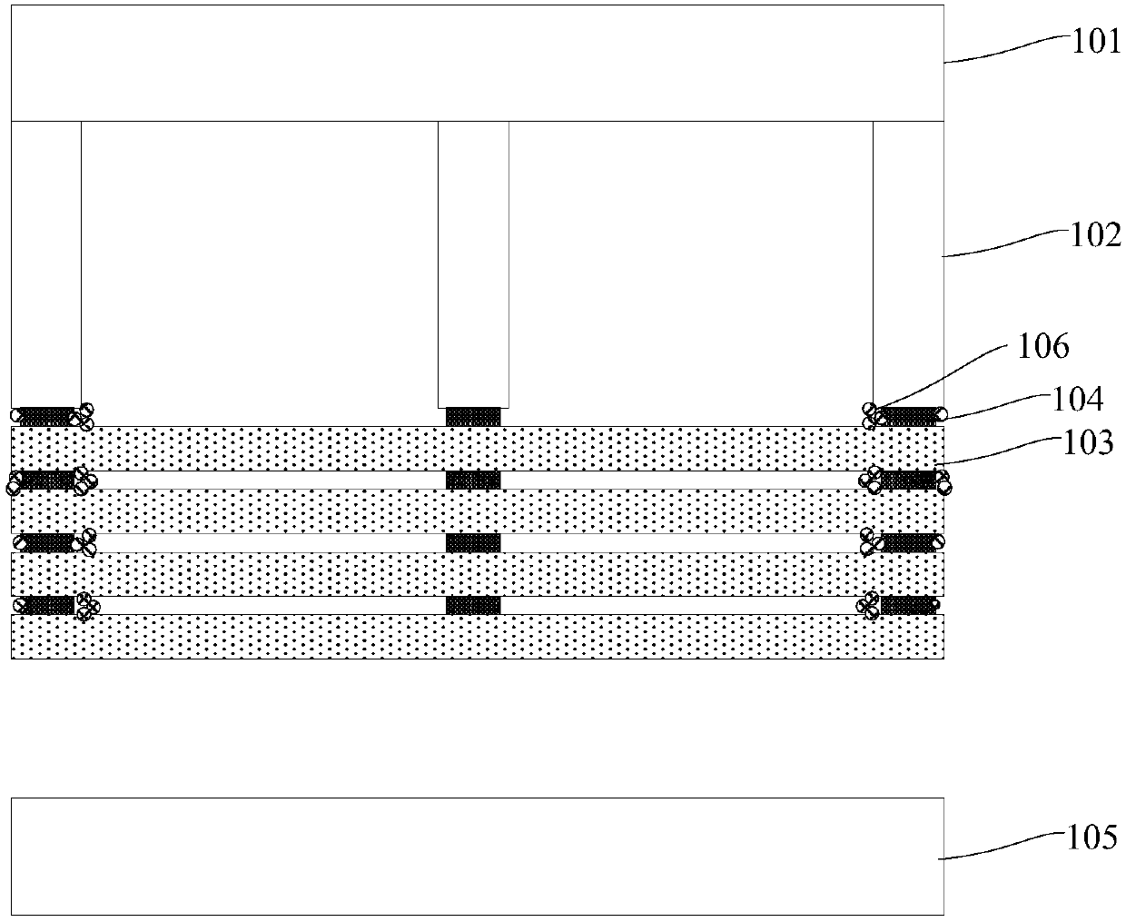
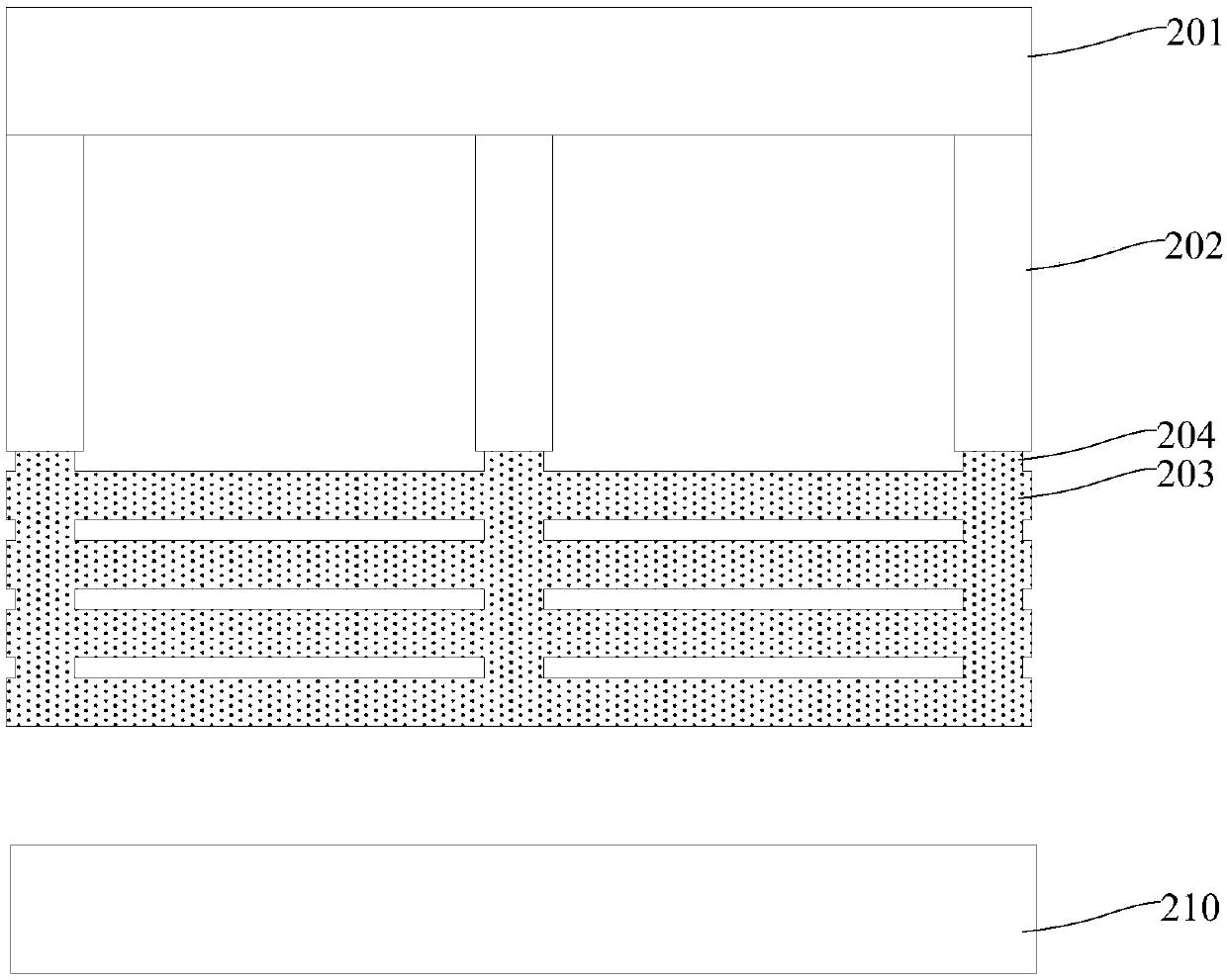
[0055] Such as Figure 3 ~ Figure 5 Shown, where, image 3 Shown as a schematic diagram of the assembly structure of the semiconductor etching equipment of this embodiment, Figure 4 A schematic diagram of the disassembly structure of the semiconductor etching equipment of this embodiment is shown, Figure 5 A cross-sectional view of the disassembled structure of the semiconductor etching equipment of this embodiment is shown. This embodiment provides a semiconductor etching equipment. The semiconductor etching equipment includes: an upper electrode spray plate 201 installed in the chamber of the semiconductor etching equipment to provide plasma gas; an annular side wall 202; The upper electrode spray plate 201; the side flow reaction element, which is connected to the annular side wall 202; and the lower electrode carrier 210, which is aligned below the side flow reaction element and is installed in the cavity of the semiconductor etching equipment Indoor; wherein, the lateral ...

Embodiment 2

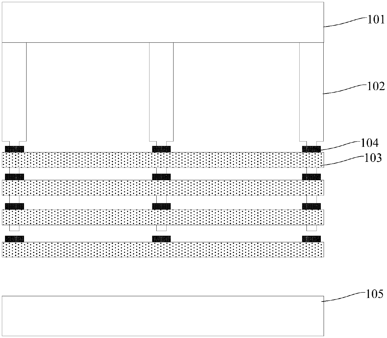
[0066] Such as Figure 6 ~ Figure 7 Shown, where, Image 6 Shown as a cross-sectional view of the disassembled structure of the semiconductor etching equipment, Figure 7 Shown is a cross-sectional view of the assembly structure of the semiconductor etching equipment. This embodiment provides a semiconductor etching equipment, the basic structure of which is the same as that of Embodiment 1. The difference from Embodiment 1 is that the quartz ring 203 has a coupling hole 208 extending laterally outward, and the annular side wall The positioning post 205 has a locking hole 206 corresponding to the position of the combining hole 208. When the positioning post 205 is combined with the positioning groove 207, the combining hole 208 and the locking hole 206 are aligned with each other and limit the position. The pin 209 is passed through to prevent the positioning column 205 from sliding relative to the positioning groove 207, that is, to prevent the lateral flow reaction element fr...

Embodiment 3

[0070] This embodiment provides a semiconductor etching equipment, the basic structure of which is the same as that of Embodiment 1. The difference from Embodiment 1 is that the bottom surface of the annular side wall 202 has a plurality of positioning grooves 207, and the quartz The ring 203 has a plurality of positioning posts 205 corresponding to the positioning grooves 207, and the positioning posts 205 are combined with the positioning grooves 207 to achieve a fixed connection between the quartz ring 203 and the annular side wall 202. Further, the annular side wall 202 has a coupling hole 208 extending laterally outward, and the positioning post 205 has a locking hole 206 corresponding to the position of the coupling hole 208. When the positioning post 205 and the positioning groove 207 are After the combination, the coupling hole 208 and the clamping hole 206 are aligned with each other and are connected by a stop pin 209 to prevent the positioning post 205 from sliding re...


PUM


Abstract

The present invention provides a semiconductor etching device comprising an upper electrode spraying disk, an annular sidewall connected to the upper electrode spraying disk, a lateral flow reaction element connected to the annular sidewall, and a lower electrode carrying table aligned under the lateral flow reaction element, wherein the lateral flow reaction element comprises at least two layersof reactive material rings and a plurality of connection parts between the reactive material rings, the connection parts are used for providing s a plurality of filtration channels at the side wall ofthe lateral flow reaction element, the reaction material rings are integrally formed with the connection parts to inhibit the adhesion of a reaction product on the lateral flow reaction element. According to the invention, the adhesion state of a reaction chamber body product of a dry etching machine can be effectively improved by integrally forming the reaction material rings and the connectingparts, the influence of the cleanliness of a wafer surface caused by the falling of the product during the movement process of the lateral flow reaction element is avoided, and the product reliabilityand yield are effectively improved.

Description

Technical field [0001] The invention belongs to the field of semiconductor equipment design and manufacturing, and particularly relates to a semiconductor etching equipment. Background technique [0002] Dry etching is a technique that uses plasma to etch thin films. When the gas exists in the form of plasma, it has two characteristics: On the one hand, the chemical activity of these gases in the plasma is much stronger than in the normal state. According to the different materials to be etched, selecting the right gas can be faster React with the material to achieve the purpose of etching and removal; on the other hand, the electric field can also be used to guide and accelerate the plasma to make it have a certain amount of energy. When it bombards the surface of the etched object, it will be etched The atoms of the material are knocked out, so as to achieve the purpose of using physical energy transfer to achieve etching. [0003] In the case of increasingly fierce competition...

Claims


Application Information

Patent Timeline
Patent Type & Authority Applications(China)
IPC IPC(8): H01L21/67H01J37/32
CPCH01J37/32853H01L21/67069
Inventor 不公告发明人
Owner CHANGXIN MEMORY TECH INC
Why Eureka
Try Eureka