Method and system for laser processing wafer

A laser processing and laser technology, used in metal processing equipment, laser welding equipment, manufacturing tools, etc., can solve the problem of slow response of the laser follower device and unable to keep up with the surface changes of the sample, to solve the adaptability problem and simplify the accuracy requirements , hardware design flexible effect

Active Publication Date: 2020-12-04
北京中科镭特电子有限公司
View PDF6 Cites 0 Cited by
  • Summary
  • Abstract
  • Description
  • Claims
  • Application Information

AI Technical Summary

Problems solved by technology

[0005] The method and system for laser processing wafers provided by the present invention can automatically adjust the height of the laser cutting head according to the undulation of the wafer surface, maintain a predetermined laser focal length, and solve the problem that the laser follower responds slowly and cannot keep up when the equipment is running at high speed The problem of sample surface changes, to achieve a processing accuracy of ±1um from the laser processing focus to the sample surface

Method used


Image

  • Method and system for laser processing wafer
  • Method and system for laser processing wafer
  • Method and system for laser processing wafer

Examples


Embodiment 1

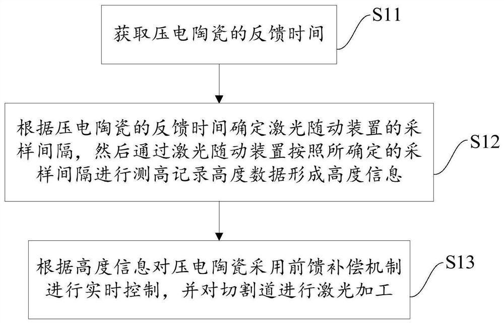
[0050] Embodiments of the present invention provide a method for laser processing wafers, such as figure 1 As shown, the method includes:

[0051] S11. Obtain the feedback time of the piezoelectric ceramic;

[0052] S12. Determine the sampling interval of the laser follower according to the feedback time of the piezoelectric ceramic, and then use the laser follower to measure and record height data according to the determined sampling interval to form height information;

[0053] S13. Real-time control of the piezoelectric ceramics with a feed-forward compensation mechanism according to the height information, and laser processing of the cutting lines.

[0054] The method for laser processing wafers provided by the embodiments of the present invention mainly compensates the slow response problem of piezoelectric ceramics (PZT) through the fast response capability of the controller; the specific technical solution is to match the optimal sampling time according to the feedback...

Embodiment 2

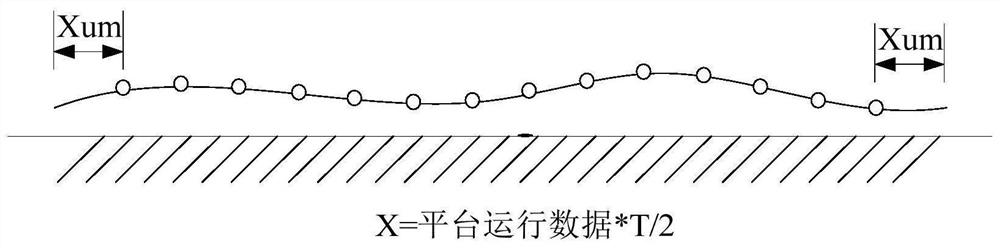
[0089] Due to the slow response of the laser servo device when the equipment is running at high speed, it cannot keep up with the change of the sample surface, and it is impossible to achieve the processing accuracy of ±1um from the change of the laser processing focus to the sample surface. Therefore, the embodiment of the present invention provides a method for laser processing wafers, such as Figure 5 As shown, the method includes:

[0090] S21. Obtain the height data of the cutting line to be processed by the laser follower;

[0091] S22. Perform data processing on the acquired height data according to the feedback time of the piezoelectric ceramics and form a positive and negative piezoelectric ceramic motion compensation table;

[0092]S23. When performing forward or reverse laser processing on the cutting line, the piezoelectric ceramics are controlled according to the forward and reverse piezoelectric ceramic motion compensation table to adopt a feedforward compensat...

Embodiment 3

[0129] Since the existing laser cutting of wafers has high requirements on the consistency of the cutting depth, the precision is at least at the micron level, but the high-speed cutting and the unevenness of the wafer surface constitute a pair of contradictory factors, and it is easy to cause the focus plane to be out of focus under the condition of high-speed movement On the wafer plane, there are breakpoints in the cutting of the wafer surface, and the frequent update of the setting value of the laser follower will also cause the oscillation error of the laser follower. Therefore, the embodiment of the present invention provides a kind of method for laser machining wafer, such as Figure 8 As shown, the method includes:

[0130] S31. Scanning the cutting line to be processed, and obtaining the height data of the cutting line by the laser follower;

[0131]S32. Fitting the height data to form a height curve of the cutting line;

[0132] S33. Determine the height setting va...


PUM


Abstract

The invention provides a laser processing method and system for a wafer. The method comprises the steps that height data of a to-be-processed cutting way are obtained through a laser servo device; according to feedback time of piezoelectric ceramics, data processing is conducted on the obtained height data, and a forward and reverse piezoelectric ceramic motion compensation table is formed; and when forward or reverse laser processing is conducted on the cutting way, the piezoelectric ceramics are controlled to conduct real-time control through a feedforward compensation mechanism according tothe forward and reverse piezoelectric ceramic motion compensation table. According to the laser processing method and system, the height of a laser cutting head can be adjusted automatically according to bumpiness of the surface of the wafer, the preset laser focal length is kept, the problems that during equipment high-speed operation, the laser servo device responds slowly and cannot follow thesample surface change are solved, and processing precision that the distance between a laser processing focus and the sample surface changes from -1 [mu]m to +1 [mu]m is achieved.

Description

technical field [0001] The invention relates to the technical field of laser processing, in particular to a method and system for laser processing wafers. Background technique [0002] In the field of semiconductor wafer processing, the industry's continuous improvement of new integrated circuit technology, product packaging capabilities, and chip performance requirements has led to thinner wafers, higher sensitivity of devices, and increasingly complex chip structures. The more complex the chip scribing process is, the more diverse the requirements are. For example, the structure of MEMS devices is very fragile, and the scribing process using high-pressure water cleaning is not allowed, nor is there any dust or particles on the surface; covered with Low -K medium chips are not allowed to peel off the film layer during scribing and also do not allow any dust or scribing debris on the surface. [0003] The first step in chip packaging is wafer dicing, and the effect of the w...

Claims


Application Information

Patent Timeline
Patent Type & Authority Patents(China)
IPC IPC(8): B23K26/53B23K26/70B23K26/064B23K26/03
CPCB23K26/032B23K26/064B23K26/53B23K26/702
Inventor 李纪东侯煜李曼张喆王然张紫辰张昆鹏易飞跃杨顺凯
Owner 北京中科镭特电子有限公司
Why Eureka
Try Eureka