Three-dimensional computing chip comprising three-dimensional memory array

A computing chip, three-dimensional storage technology, applied in electrical components, electrical solid-state devices, circuits, etc., can solve problems such as disadvantage of high-performance computing of processors, unsuitable for massive computing parameters, and slow external memory.

Inactive Publication Date: 2019-03-29
CHENGDU HAICUN IP TECH
View PDF7 Cites 3 Cited by
  • Summary
  • Abstract
  • Description
  • Claims
  • Application Information

AI Technical Summary

Problems solved by technology

However, the speed of these external memories is relatively slow, which is not suitable for reading massive calculation parameters, which is very unfavorable f

Method used


Image

  • Three-dimensional computing chip comprising three-dimensional memory array
  • Three-dimensional computing chip comprising three-dimensional memory array
  • Three-dimensional computing chip comprising three-dimensional memory array

Examples


Embodiment Construction

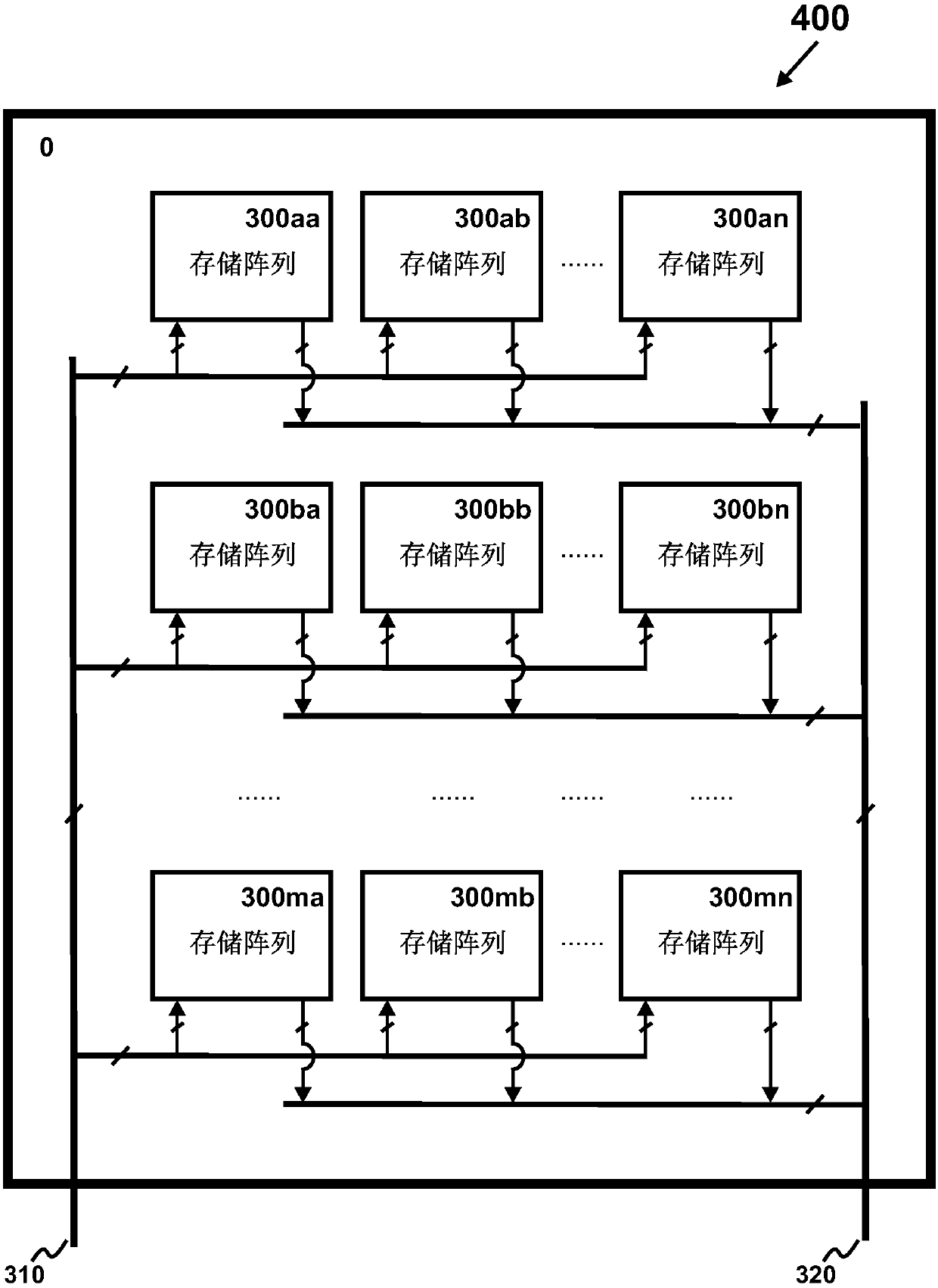
[0025] Figure 3AIt represents a three-dimensional computing (3D-COM) chip 200 , which stores massive computing parameters in the 3D-M array 170 inside the chip 200 . The 3D-COM chip 200 is formed in a semiconductor substrate 0 , which contains m x n storage units 100aa-100mn, and the storage unit is the smallest repeating unit of the 3D-COM chip 200 . Each storage unit is electrically coupled to an input 110 and an output 120 . Note that a 3D-COM chip 200 may contain thousands of storage units 100aa-100mn. For example, a 3D-COM chip 200 with a storage capacity of 128Gb contains 64,000 storage units. A large number of storage units guarantee ultra-large-scale parallel computing.

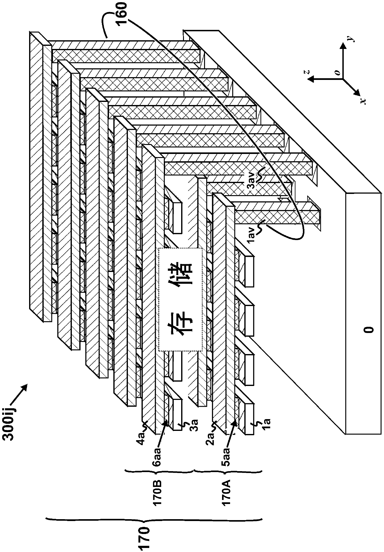
[0026] Figure 3B The structure of the storage unit 100ij is shown from another angle. Each storage unit includes a micro-computing core 180 and at least one 3D-M array 170 . A microcomputing core 180 is formed in substrate 0, which contains the computational logic. The 3D-M array 170 is stack...


PUM


Abstract

The invention proposes a three-dimensional computing (3D-COM) chip comprising a three-dimensional memory (3D-M) array. Unlike the traditional storage of computational data, the 3D-M array in the 3D-COM is mainly used for storing memory parameters. One 3D-COM chip comprises thousands of memory and computing units. Each memory and computing unit implements three-dimensional integration between the 3D-M array and a computational core at a microscale, and realizes ultra-large-scale parallel computing.

Description

technical field [0001] The invention relates to the field of integrated circuits, more specifically, to a processor chip containing a three-dimensional memory array, that is, a three-dimensional computing chip. Background technique [0002] US Patent 5,835,396 (inventor: Zhang Guobiao; date of authorization: November 10, 1998) and Chinese patent 98119572.5 (inventor: Zhang Guobiao; date of authorization: January 22, 2003) disclose a three-dimensional memory ( three-dimensional memory, referred to as 3D-M). Figure 1A It is a layout diagram of a 3D-M chip; Figure 1B is a perspective view of a 3D-M array in 3D-M. Each 3D-M chip 300 is formed on a semiconductor substrate 0, which contains a plurality of 3D-M arrays 300aa-300mn. The 3D-M array is the smallest repeating unit of the 3D-M chip ( Figure 1A ). The input 310 of the 3D-M chip 300 is address and / or input data, and the output 320 is output data. Each 3D-M array 300ij contains a plurality of vertically stacked memor...

Claims


Application Information

Patent Timeline
IPC IPC(8): H01L27/06
CPCH01L27/0688
Inventor 张国飙
Owner CHENGDU HAICUN IP TECH
Why Eureka
Try Eureka