Crystal particle method and system

A detection system and die technology, applied in semiconductor/solid-state device testing/measurement, electrical components, circuits, etc., can solve the problems of inability to control the panel die defect rate, difficult die electrical testing, and difficulty in detection.

Inactive Publication Date: 2019-04-05
AU OPTRONICS CORP
View PDF7 Cites 1 Cited by
  • Summary
  • Abstract
  • Description
  • Claims
  • Application Information

AI Technical Summary

Problems solved by technology

However, when the grain size is as small as the size of the probe, such as: micro LED (micro LED), it is difficult to use the detection method of the existing technology to conduct electrical tests on the grain
[0003] Therefore, micro-LEDs in the prior art usually transfer the dies to the panel through a micro transfer printing process after the dies are diced on the source wafer, and the die defect rate of the panel cannot be controlled.
For this reason, the existing grain detection methods are difficult to apply to small-scale grains, which makes detection of small-scale grains difficult, so the existing grain detection methods still have shortcomings and there is room for improvement

Method used


Image

  • Crystal particle method and system
  • Crystal particle method and system
  • Crystal particle method and system

Examples


no. 1 example

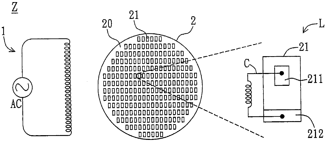
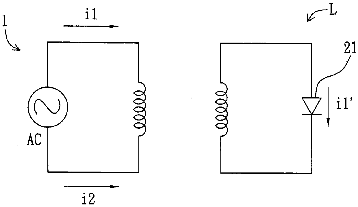
[0048] The following fit Figure 1 to Figure 3 The grain inspection system and method of the first embodiment of the present invention will be described. please see figure 1 , this embodiment provides a die inspection system Z, which has a coil 1 and a source wafer 2 . The aforementioned "source wafer" includes but is not limited to a silicon chip on which the die 21 is grown. The upper surface 20 of the source wafer 2 has a plurality of dies 21 . In this embodiment, the die 21 is a micro LED die, however, the present invention is not limited thereto; in other embodiments, the die 21 can be other types of semiconductor die.

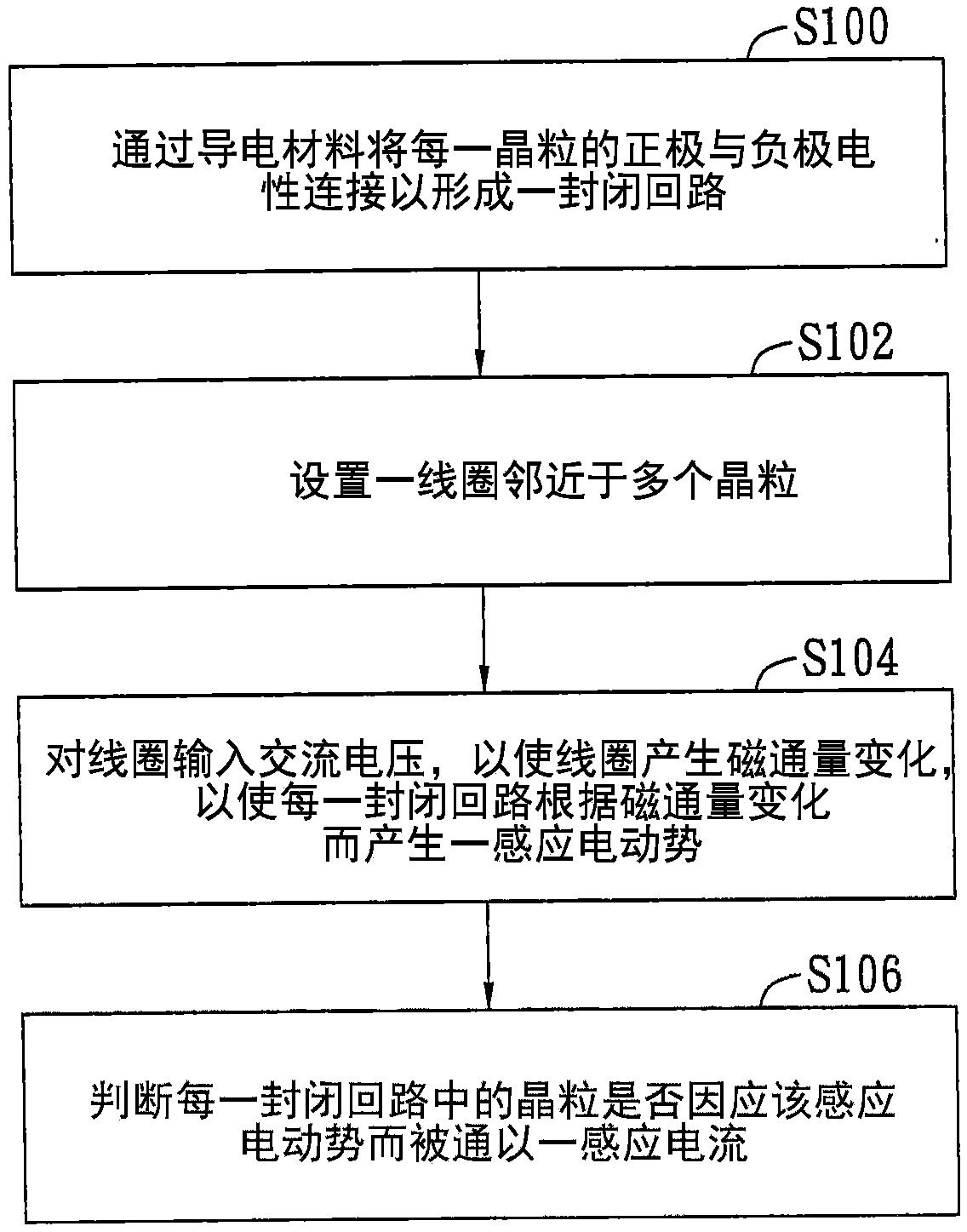
[0049] Please refer to figure 1 and figure 2 , this embodiment provides a grain inspection method using the grain inspection system Z, the grain inspection method at least includes the following steps. Step S100: Electrically connect the positive electrode 211 and the negative electrode 212 of each crystal grain 21 through a conductive material C t...

no. 2 example

[0058] The following fit Figure 6 to Figure 17 The grain inspection system Z and the grain inspection method provided by the second embodiment of the present invention will be described. See first Image 6 , the die detection system Z provided in this embodiment includes at least one coil 1 and a source wafer 2 . In this embodiment, among the plurality of dies 21 on the source wafer 2, every two adjacent dies 21 form a die pair 210, and each die pair 210 includes a first die 21A and a second die grain 21B.

[0059] The following fit Image 6 and Figure 7 The grain inspection method of the second embodiment is described, which uses the above-mentioned grain inspection system Z and includes at least the following steps. Step S200: Form a closed circuit between the first crystal grain 21A and the second crystal grain 21B of each crystal grain pair 210 through a conductive material, wherein the first crystal grain 21A in each crystal grain pair 210 is connected with the pos...


PUM


Abstract

The invention provides a crystal grain detection method and system for detecting crystal grains on a source wafer. The grain detection method comprises the following steps: electrically connecting a positive electrode and a negative electrode of each grain through a conductive material to form a closed loop; disposing a coil adjacent to the plurality of dies; inputting an alternating voltage to the coil to change the magnetic flux of the coil, generating an induced electromotive force by each closed loop according to the change of the magnetic flux, and enabling the peak value of the induced electromotive force to be higher than the breakover voltage of the crystal grain; and judging whether the crystal grains in each closed loop are conducted with induced current due to induced electromotive force or not.

Description

technical field [0001] The invention relates to a grain detection method and system, in particular to a grain detection method and system for detecting grains on a source wafer. Background technique [0002] The traditional wafer inspection method is to use a probe with a diameter of about 10 μm to contact the contacts on the die for electrical testing. When the dies are inspected to be flawless, subsequent processes such as dicing, sorting, and packaging are carried out. However, when the size of the crystal grain is as small as the size of the probe, such as micro LED, it is difficult to use the detection method of the prior art to conduct an electrical test on the crystal grain. [0003] Therefore, the micro-LEDs in the prior art usually transfer the dies to the panel through a micro transfer printing process after the dies are diced on the source wafer, and the die defect rate of the panel cannot be controlled. For this reason, the existing grain inspection methods are...

Claims


Application Information

Patent Timeline
Patent Type & Authority Applications(China)
IPC IPC(8): H01L21/66
CPCH01L22/12
Inventor 奚鹏博林振祺
Owner AU OPTRONICS CORP
Why Eureka
Try Eureka