Multi-path reflection fluorescent probe

A technology of multiple reflection and fluorescence probes, applied in fluorescence/phosphorescence, Raman/scattering spectroscopy, optical radiation measurement, etc., can solve problems such as use restrictions, errors, and low resolution

Inactive Publication Date: 2009-07-15
IND TECH RES INST
View PDF3 Cites 0 Cited by
  • Summary
  • Abstract
  • Description
  • Claims
  • Application Information

AI Technical Summary

Problems solved by technology

In addition, since the automatic optical inspection machine based on the fluorescent signal is not sensitive to the oxidized metal area on the circuit board, it will not cause false calls (False Calls) due to metal oxidation points, but the automatic optical inspection machine with reflective white light The detection system cannot distinguish the oxidized part of the metal, which leads to wrong judgment of circuit defects, and because the reflective white light automatic optical detection system has strong light intensity but low resolution, resulting in restrictions on its use. induced fluorescence for detection
[0005] At present, the structure of optical detection instruments mostly uses fluorescent probes with single or multiple light sources, which are imaged on the image detector through the assembly of optical mirrors, such as Image 6 As shown, it is an optical detection instrument with a double light source 70, the excitation light reaches the substrate 60 through the reflection of the mirror group 80, and finally transmits to the image detector 90, but under the structure of this instrument, the light emitted by the light source Most of them diverge and are not sent to the image detector, resulting in insufficient light intensity

Method used


Image

  • Multi-path reflection fluorescent probe
  • Multi-path reflection fluorescent probe
  • Multi-path reflection fluorescent probe

Examples


Embodiment 1

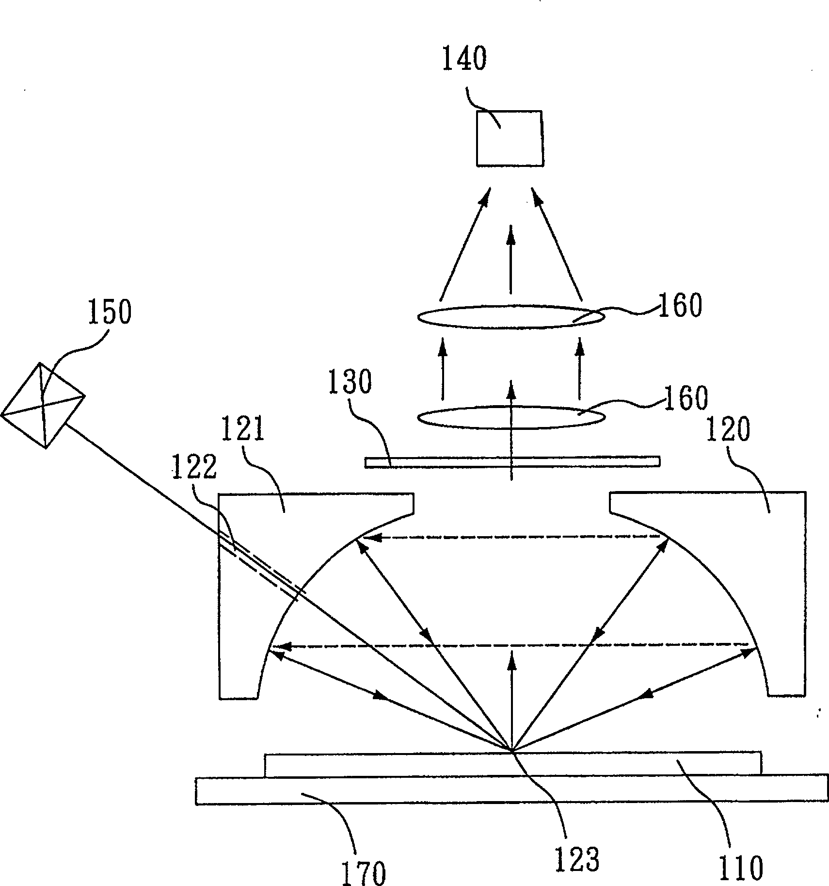
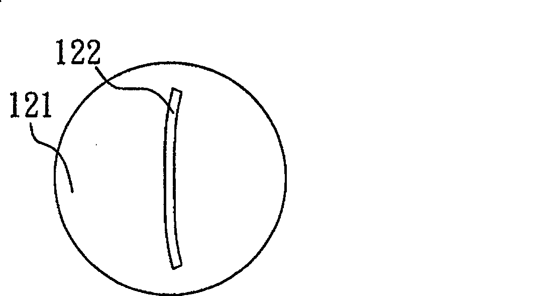
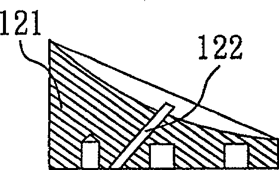
[0021] For the multiple reflection fluorescence probe in this example, see figure 1 , is to cooperate with a defect detection on the surface of a printed circuit board 110, using laser to excite the organic fluorescent material of the non-metal wire part, cooperate with the optical filter 130 to filter the excitation laser, and then use the image detector 140 to retrieve its laser induced fluorescence (Laser Induced Fluorescence) Fluorescence, LIF) images. The multiple reflection fluorescence probe includes two off-axis parabolic mirrors 120 and 121 confocally arranged, and its shape is as follows: Figure 2(A) to 2(D) As shown, one of the off-axis parabolic mirrors 121 has a linear slit 122 inclined at 45 degrees; a linear laser light source 150 generates laser excitation light, and directly incident off-axis through the linear slit 122 at an angle of 45 degrees The focus 123 position of the parabolic mirrors 120 and 121; an image detector 140, to detect the fluorescence in...

Embodiment 2

[0023] For the multiple reflection fluorescence probe in this example, see image 3 , is to cooperate with the defect detection on the surface of a printed circuit board 210, using laser to excite the organic fluorescence of the non-metal wire part, cooperate with the optical filter 230 to filter the laser, and then use the image detector 240 to retrieve the laser induced fluorescence (Laser Induced Fluorescence) , LIF) images. The reflective fluorescence probe includes two off-axis parabolic mirrors 220 and 221 confocally arranged, wherein one off-axis parabolic mirror 221 has a linear slit 222 parallel to the surface of the printed circuit board 210; a linear laser light source 250 generates laser excitation light, and pass through the linear slit 222, reach the off-axis parabolic mirror 221, and then reflect to the focal point 223 position of the off-axis parabolic mirror; an image detector 240, to detect the fluorescence induced by the fluorescent material on the printed c...

Embodiment 3

[0025] For the multiple reflection fluorescence probe in this example, see Figure 4, is matched with a biochip 310 implanted with nucleic acid probes of a plurality of fluorescent groups, which is excited by laser, and cooperates with a dichroic mirror 330 to filter out the exciting laser light, and then uses an image detector 340 to retrieve its laser-induced fluorescence image . The fluorescence probe includes two off-axis parabolic mirrors 320 and 321 confocally arranged; a linear laser light source 350 generates laser excitation light, which is reflected by a dichroic mirror 330 and reaches the focal point 323 of the off-axis parabolic mirror; an image detection A device 340, to detect the position of the fluorescent substance; a dichroic mirror 330, located between the biochip 310 and the image detector 340, to filter the excitation light of the laser, so that the fluorescence can penetrate and reach the image detector 340; A detection platform 370 that moves horizontal...


PUM

PropertyMeasurementUnit
angle of incidenceaaaaaaaaaa

Abstract

The multiple fluorescence reflecting probe for the fluorescent material detection of sample surface includes one light source to generate exciting light, which irradiates the fluorescent material on the sample to produce fluorescence; two confocal off-axis paraboloidal mirrors to collect and reflect the exciting light and fluorescence incident to the sample; one image detector to detect the fluorescence the fluorescent material in the sample generates; one light filtering lens between the sample and the image detector to filter off the reflected exciting light; and one optical developing lens set located between the light filtering lens and the image detector to focus the fluorescence onto the image detector.

Description

technical field [0001] The invention relates to a multiple reflection fluorescence probe, in particular to a multiple reflection fluorescence probe suitable for a printed circuit board or a biological wafer. Background technique [0002] There are two types of automatic optical inspection of printed circuit board (PCB): 1. Use white light (White Light) 10 to irradiate printed circuit board 20, and then use light sensor detector 30 to retrieve the reflected light signal of its metal wire , and become a reflection image after image processing, such as Figure 5 shown. 2. Use laser to excite the organic fluorescent substrate of the non-metal wire part, and then use the photosensitive detector to retrieve the laser-induced fluorescence (Laser Induced Fluorescence, LIF) image. [0003] The biggest difference between the above-mentioned automatic optical inspection methods lies in their optical illumination system. The first method uses white light to irradiate the printed circui...

Claims


Application Information

Patent Timeline
Patent Type & Authority Patents(China)
IPC IPC(8): G01N21/88G01N21/64
CPCG01J2003/1213G01J3/0208G01N21/6456G01J3/0243G01J3/0218G01J3/4406G01J3/0227G01N2021/6463G01N21/645G01J3/02
Inventor 李耀昌林雁容刘定坤
Owner IND TECH RES INST
Why Eureka
Try Eureka