Forming method of semiconductor device and semiconductor device

A technology for semiconductors and devices, applied in the field of semiconductors, can solve problems such as breakdown over time, no reduction in capacitance, reliability risks, etc.

Inactive Publication Date: 2019-04-05
YANGTZE MEMORY TECH CO LTD
View PDF2 Cites 2 Cited by
  • Summary
  • Abstract
  • Description
  • Claims
  • Application Information

AI Technical Summary

Problems solved by technology

[0004] However, using low-k oxide as a dielectric layer is more likely to cause reliability risks, such as time-dependent breakdown (TimeDependent Dielectric Breakdown, TDDB), leakage current, stress migration (Stress Migration, SM), and will not provide such as much capacit

Method used


Image

  • Forming method of semiconductor device and semiconductor device
  • Forming method of semiconductor device and semiconductor device
  • Forming method of semiconductor device and semiconductor device

Examples


Embodiment 1

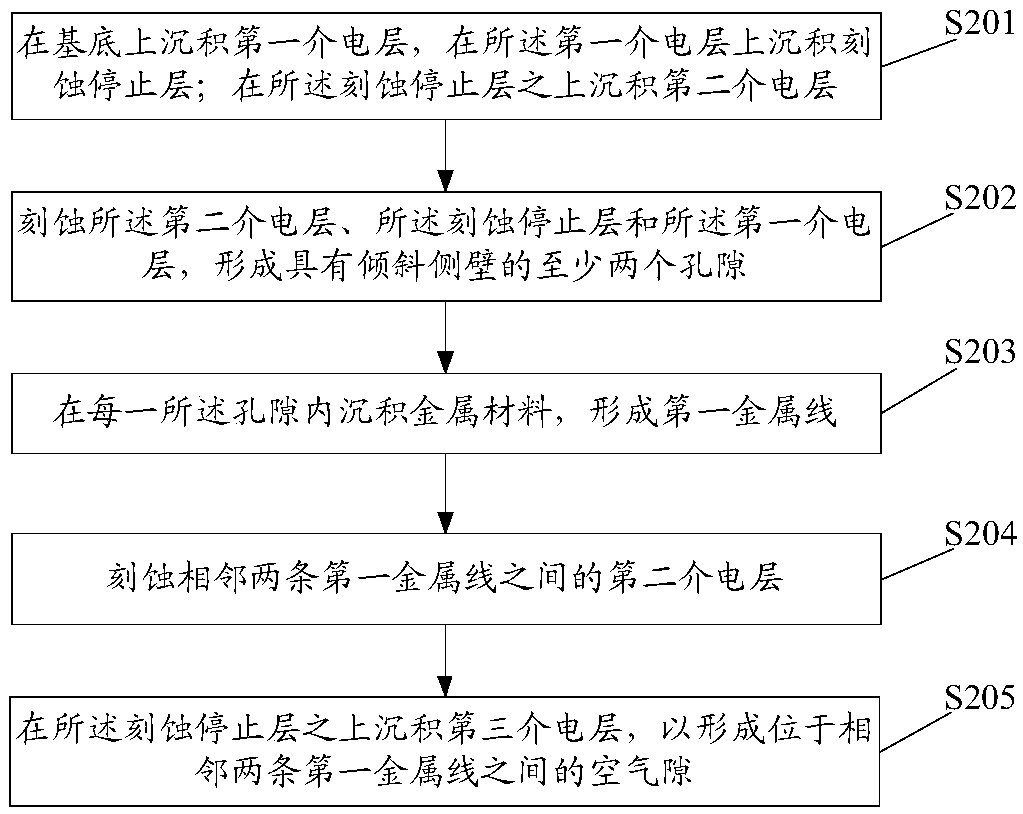
[0069] Based on the above-mentioned problems in the related art, the present embodiment provides a method for forming a semiconductor device. The method for forming a semiconductor device can facilitate the pinch-off of the air gap at the top by forming the first metal line with inclined sidewalls. An effective air gap is formed, thereby improving the RC delay of the semiconductor device.

[0070] figure 2 It is a schematic diagram of the implementation flow of the method for forming a semiconductor device provided in the embodiment of the present application, as shown in figure 2 As shown, the method includes the following steps:

[0071] Step S201 , depositing a first dielectric layer on the substrate, depositing an etching stop layer on the first dielectric layer; depositing a second dielectric layer on the etching stop layer.

[0072] Such as Figure 3A As shown, a first dielectric layer 31 is deposited on a substrate 30, an etch stop layer 32 is deposited on the firs...

Embodiment 2

[0101] This embodiment provides a method for forming a semiconductor device. By forming a first metal line with an inclined sidewall, the method for forming a semiconductor device can facilitate the pinching of the air gap at the top to form an effective air gap, thereby improving the semiconductor performance. RC delay of the device.

[0102] Figure 4 It is a schematic diagram of the implementation flow of the method for forming a semiconductor device provided in the embodiment of the present application, as shown in Figure 4 As shown, the method includes the following steps:

[0103] Step S401, providing a substrate, and depositing a first dielectric layer on the substrate.

[0104] Such as Figure 5A As shown, a first dielectric layer 52 is deposited on a substrate 51, and there are at least two second metal lines 521 in the first dielectric layer 52, and the extending direction of each second metal line 521 is perpendicular to the The first dielectric layer 52 .

[...

Embodiment 3

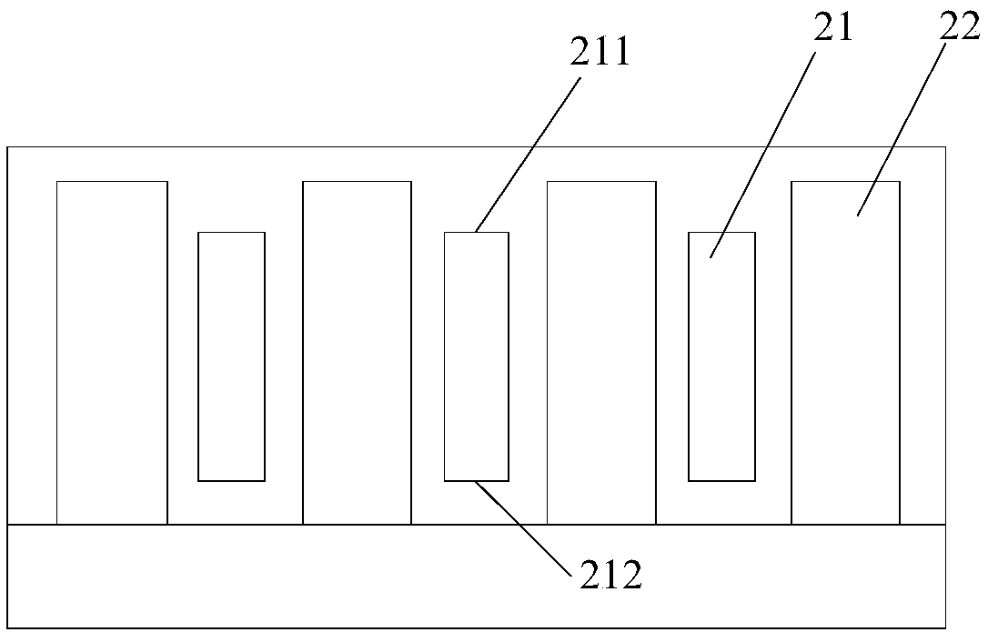
[0153] An embodiment of the present application provides a semiconductor device. In this embodiment, the semiconductor device may be a NAND flash memory.

[0154] Figure 6 A schematic structural diagram of a semiconductor device provided in the embodiment of the present application, such as Figure 6 As shown, the semiconductor device includes:

[0155] base 60;

[0156] a first dielectric layer 61 on the substrate;

[0157] an etch stop layer 62 over the first dielectric layer;

[0158] at least two apertures 611 with sloped sidewalls;

[0159] a first metal line 612 located within each of said apertures;

[0160] a third dielectric layer 63 deposited over the etch stop layer;

[0161] The air gap 613 is located between two adjacent first metal lines.

[0162] Here, the substrate 60 is located at the bottom of the entire semiconductor device, and the material of the substrate 60 can be selected from one of Si, SiGe, SiC, Al2O3, AlN, ZnO, Ga2O3, LiAlO2 and the like. S...


PUM


Abstract

The embodiment of the invention discloses a forming method of a semiconductor device and a semiconductor device. The method comprises steps: depositing a first dielectric layer on a substrate, and depositing an etching stop layer on the first dielectric layer; depositing a second dielectric layer on the etching stop layer; etching the second dielectric layer, the etching stop layer and the first dielectric layer to form at least two pores with inclined side walls; depositing a metal material in each hole to form a first metal line; Etching the second dielectric layer between two adjacent firstmetal wires; a third dielectric layer is deposited over the etch stop layer to form an air gap between two adjacent first metal lines.

Description

technical field [0001] Embodiments of the present invention relate to the field of semiconductor technology, and relate to, but are not limited to, a method for forming a semiconductor device and the semiconductor device. Background technique [0002] With the further development of computer flash memory devices (NAND), the performance requirements for NAND flash memories are getting higher and higher, for example, resistance-capacitance (Resistance-Capacitance, RC) delay. [0003] In the prior art, a low-k oxide with a low dielectric constant (low-k) is usually used as the dielectric layer in the back-end of the line (BackEnd of Line, BEOL) metal interconnection to reduce the RC delay; or, use Dry etching removes the oxide of the dielectric layer to form an air gap. Since the k value of air is much lower than that of oxide (the k value of air is about 1, and the k value of oxide is about 3.9), it can improve RC delay of metal lines. [0004] However, using low-k oxide as ...

Claims


Application Information

Patent Timeline
IPC IPC(8): H01L21/768H01L23/528
CPCH01L21/7682H01L21/76838H01L23/528
Inventor 袁璐月刘峻
Owner YANGTZE MEMORY TECH CO LTD
Why Eureka
Try Eureka