Supercharge Your Innovation With Domain-Expert AI Agents!

Method for fabricating interconnection structure

A technology of interconnect structure and manufacturing method, which is applied in semiconductor/solid-state device manufacturing, electrical components, circuits, etc., and can solve the problems of semiconductor substrate stress mismatch, trench disconnection, etc.

Inactive Publication Date: 2019-04-05
SHANGHAI HUALI MICROELECTRONICS CORP
View PDF2 Cites 0 Cited by
  • Summary
  • Abstract
  • Description
  • Claims
  • Application Information

AI Technical Summary

Problems solved by technology

[0004] The purpose of the present invention is to provide a method for manufacturing an interconnection structure to solve the problem of trench disconnection caused by the stress mismatch of the semiconductor substrate in the prior art

Method used


Image

  • Method for fabricating interconnection structure
  • Method for fabricating interconnection structure
  • Method for fabricating interconnection structure

Examples


Embodiment Construction
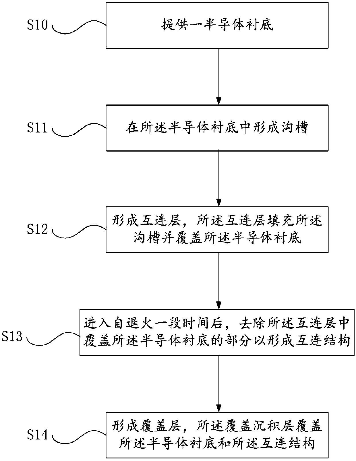
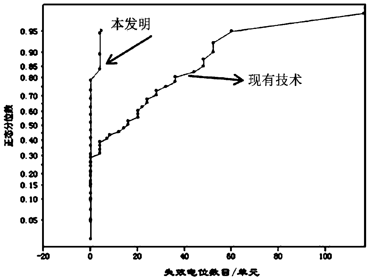
[0029] The core idea of ​​the present invention is to provide a manufacturing method of an interconnect structure, which has no new process and can change the growth rate of copper grains without affecting the production capacity of the factory, so as to solve the problem of semiconductor lining in the prior art. The problem of trench disconnection caused by the mismatch of bottom stress improves product yield and process reliability.

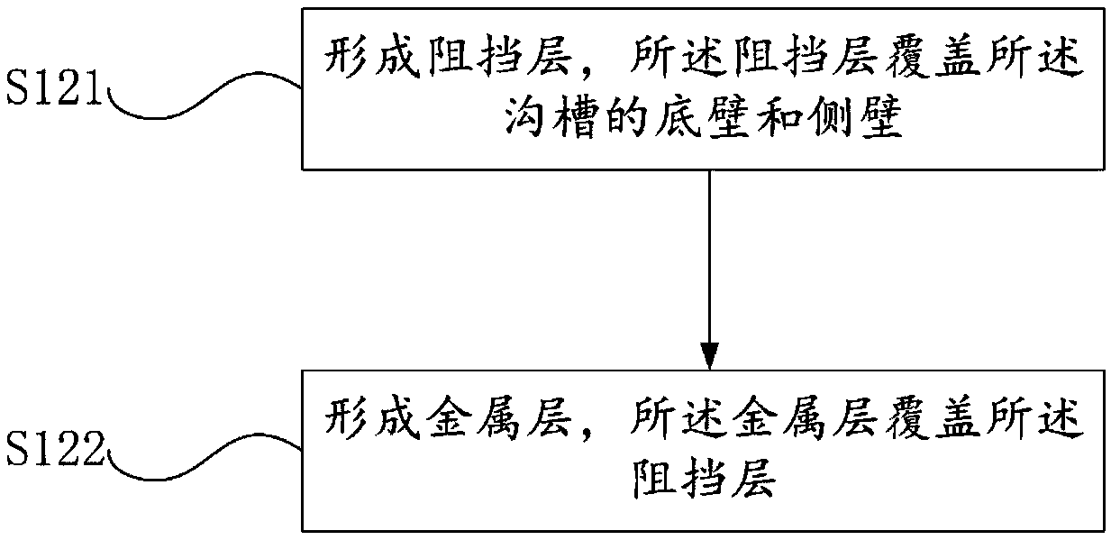
[0030] In order to realize the above-mentioned idea, the present invention provides a manufacturing method of an interconnect structure, the manufacturing method of the interconnect structure includes: providing a semiconductor substrate; forming a trench in the semiconductor substrate; forming an interconnect layer, so that the The interconnection layer fills the trenches and covers the semiconductor substrate; after entering the self-annealing period for a period of time, the part of the interconnection layer covering the semiconductor substra...


PUM

PropertyMeasurementUnit
Section widthaaaaaaaaaa

Abstract

The present invention provides a method for fabricating an interconnection structure. The method comprises providing a semiconductor substrate; forming a trench in the semiconductor substrate; formingan interconnection layer to fill the trench and cover the semiconductor substrate; after self-annealing is performed for a period of time, removing a portion of the interconnection layer covering thesemiconductor substrate to form the interconnection structure; and forming a covering layer to cover the semiconductor substrate and the interconnection structure, wherein the period of time is in arange of 1h to 10h. Since the grain size on the semiconductor substrate has a self-annealing phenomenon at room temperature, the self-annealing is performed after the interconnection layer is formed,and then the interconnection layer is removed and the covering layer is formed after 1h to 10h. Though the self-annealing takes a longer time than the rapid annealing, the interconnection layer can achieve stress matching in the small-sized trench to avoid a peeling phenomenon, thereby avoiding the problem of semiconductor line disconnection and ensuring the yield of the semiconductor products.

Description

technical field [0001] The present invention relates to the technical field of semiconductor manufacturing processes, and in particular, to a manufacturing method of an interconnect structure. Background technique [0002] As the size of semiconductor devices continues to decrease, the fabrication of interconnect structures also faces enormous challenges. Among them, interconnect refers to wires supported by conductive materials such as aluminum, polysilicon or copper that transmit electrical signals to different parts of the chip. Interconnects are also used as common metal connections between on-chip devices and the entire package. In addition to the problems of process uniformity and filling difficulties, small-sized metal connections / trenches also face the problem of disconnection caused by stress mismatch in the manufacturing process, which affects local stress, such as metal / dielectric properties, electroplating, etc. Liquid impurities, plating speed and annealing pr...

Claims


Application Information

Patent Timeline
IPC IPC(8): H01L21/768
CPCH01L21/76882H01L21/76883
Inventor 林爱梅
Owner SHANGHAI HUALI MICROELECTRONICS CORP
Features
  • R&D
  • Intellectual Property
  • Life Sciences
  • Materials
  • Tech Scout
  • Unparalleled Data Quality
  • Higher Quality Content
  • 60% Fewer Hallucinations
Learn More