Pixel definition layer, ink-jet printing method, display substrate and preparation method thereof and display device
A pixel-defining layer and pixel-defining technology, applied in semiconductor/solid-state device manufacturing, electrical components, electrical solid-state devices, etc., can solve the problems of uneven display brightness, uneven shape, and influence on the display effect of organic light-emitting display devices in the pixel area. , to achieve the effect of being conducive to narrow frame design, uniform shape, and reducing space size
- Summary
- Abstract
- Description
- Claims
- Application Information
AI Technical Summary
Problems solved by technology
Method used
Image

Examples
preparation example Construction
[0036]At least one embodiment of the present disclosure provides a method for preparing a display substrate. The display substrate includes a display region and a peripheral region. The method includes: forming the above-mentioned pixel defining layer, wherein the display pixel defining region and the auxiliary pixel defining region of the pixel defining layer Corresponding to the display area and the peripheral area respectively; a plurality of first pixels are formed in the display area by a plurality of first pixel defining units, and a plurality of second pixels are formed in the peripheral area by a plurality of second pixel defining units.
[0037] At least one embodiment of the present disclosure provides a display device, including the above-mentioned display substrate.
Embodiment 1
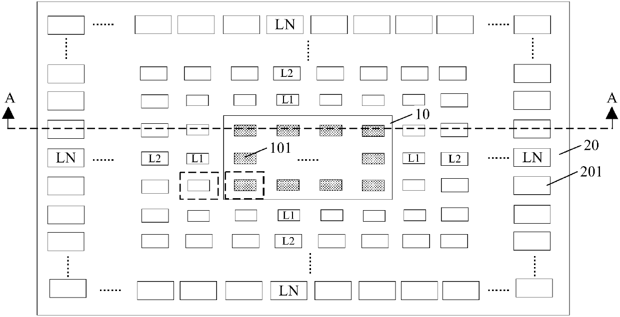
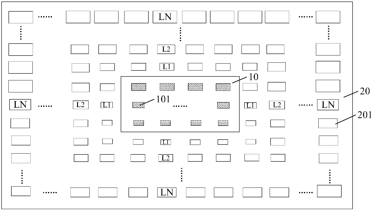
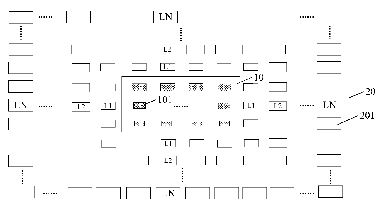
[0040] The present embodiment provides a pixel defining layer, which can be used to form an array substrate such as an organic light emitting diode (OLED) display panel. Such as figure 1 As shown, the pixel defining layer includes a display pixel defining region 10 and an auxiliary pixel defining region 20 surrounding the display pixel defining region 10; the display pixel defining region 10 includes a plurality of first pixel defining units 101; the auxiliary pixel defining region 20 includes a plurality of The second pixel defining unit 201 , and the opening area of at least part of the second pixel defining unit 201 is larger than the opening area of the first pixel defining unit 101 .
[0041] In this example, if figure 1 As shown, the first pixel defining unit and the second pixel defining unit may be arranged in a matrix form, for example, a plurality of pixel defining units form rows and columns and are aligned with each other. For example, a plurality of second p...
Embodiment 2
[0057] This embodiment provides a method for inkjet printing using the pixel defining layer provided in the above embodiment, which can be used to form an array substrate such as an OLED display panel, and the method includes: forming the first pixel defining unit and the second pixel Inkjet printing is carried out within the openings defining the cells, thereby forming the desired functional layer.
[0058] For example, in this embodiment, when inkjet printing is performed, the amount of ink jet printed in the opening of the second pixel defining unit may be more than the amount of ink jet printing in the opening of the first pixel defining unit. For example, the amount of ink jet printed in the second pixel defining unit and the first pixel defining unit may be proportional to the size of the openings of the second pixel defining unit and the first pixel defining unit respectively. Therefore, by inkjet printing different amounts of ink in the pixel defining units with differ...
PUM
 Abstract
Description
Claims
Application Information
 - R&D
- Intellectual Property
- Life Sciences
- Materials
- Tech Scout
- Unparalleled Data Quality
- Higher Quality Content
- 60% Fewer Hallucinations
Browse by: Latest US Patents, China's latest patents, Technical Efficacy Thesaurus, Application Domain, Technology Topic, Popular Technical Reports.
© 2025 PatSnap. All rights reserved.Legal|Privacy policy|Modern Slavery Act Transparency Statement|Sitemap|About US| Contact US: help@patsnap.com