Miniaturized double-layer half-mode substrate integrated waveguide six-port device

A technology of half-mode substrate integration and substrate-integrated waveguide, which is applied in the field of miniaturized double-layer half-mode substrate-integrated waveguide devices, can solve the problems of limiting the scope of application of six ports, difficulty in integration, and large volume, and achieves easy-to-understand, The effect of reducing processing difficulty and widening working bandwidth

Active Publication Date: 2021-07-13
NANJING UNIV OF POSTS & TELECOMM
View PDF2 Cites 0 Cited by
  • Summary
  • Abstract
  • Description
  • Claims
  • Application Information

AI Technical Summary

Problems solved by technology

As a transceiver in a communication system, the six-port is also widely used in various modulation and demodulation systems, but the traditional waveguide six-port device has a three-dimensional structure, large volume, and is not easy to integrate, and the traditional substrate The integrated waveguide six-port device is also mainly a single-layer circuit board. This structure has the same shortcomings as above, and these shortcomings greatly limit the scope of application of the six-port

Method used


Image

  • Miniaturized double-layer half-mode substrate integrated waveguide six-port device
  • Miniaturized double-layer half-mode substrate integrated waveguide six-port device
  • Miniaturized double-layer half-mode substrate integrated waveguide six-port device

Examples


Embodiment Construction

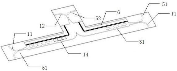
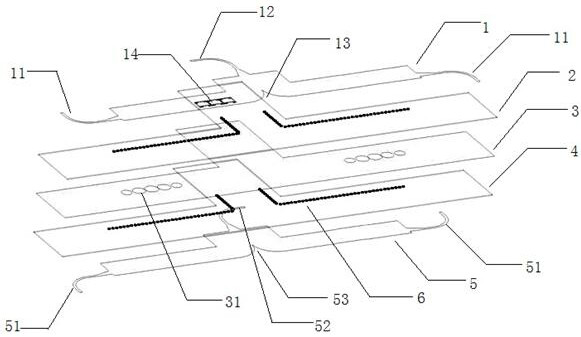
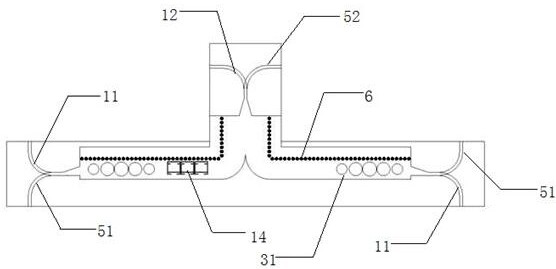
[0030] Miniaturized double-layer half-mode substrate integrated waveguide six-port device, such as Figure 1-Figure 3 As shown, it includes a top layer dielectric substrate 2, a bottom layer dielectric substrate 4, and an intermediate layer metal layer 3 arranged between them that are stacked and attached to each other. The upper surface of the top layer dielectric substrate 2 is provided with a top layer metal layer. 1. The lower surface of the underlying dielectric substrate 4 is provided with an underlying metal layer 5 .

[0031] Wherein, the top dielectric substrate 2 and the bottom dielectric substrate 4 are provided with two groups of mutually symmetrical metallized through holes 6, each group of metallized through holes 6 includes two rows of metallized through holes 6, and two rows of metallized through holes 6 The through hole 6 is "L"-shaped; the two groups of metallized through holes 6 on the top dielectric substrate 2, the top metal layer 1, the top dielectric sub...


PUM

PropertyMeasurementUnit
thicknessaaaaaaaaaa
frequencyaaaaaaaaaa

Abstract

The invention discloses a miniaturized double-layer half-mode substrate integrated waveguide six-port device, which includes a top layer dielectric substrate, a bottom layer dielectric substrate, and a middle layer metal layer that are stacked and attached to each other, and the upper surface of the top layer dielectric substrate is arranged There is a top metal layer, and the lower surface of the bottom dielectric substrate is provided with a bottom metal layer; the top dielectric substrate and the bottom dielectric substrate are provided with two sets of mutually symmetrical metallized through holes, and a set of metallized through holes is connected to the top metal layer. 1. The top dielectric substrate and the middle layer metal layer constitute the first half-mode substrate integrated waveguide; a group of metallized through holes and the bottom metal layer, the bottom dielectric substrate and the middle layer metal layer constitute the second half-mode substrate integrated waveguide; The top metal layer is provided with three ports and multiple complementary split resonant rings; the middle metal layer is provided with two rows of mutually symmetrical round holes; the bottom metal layer is provided with three ports. The invention has the advantages of simple design structure, wide six-port stable output working bandwidth, compact structure, reduced processing difficulty and cost, and reduced volume.

Description

technical field [0001] The invention relates to a miniaturized double-layer half-mode substrate integrated waveguide device, in particular to a miniaturized double-layer half-mode substrate integrated waveguide six-port device, which belongs to the field of microwave technology. Background technique [0002] Six-port technology was first used to measure the complex reflection coefficient of microwave circuits. With the further development of science and technology, six-port devices have been more widely used in power measurement systems and receiver systems. The performance of the six ports directly affects the accuracy of the entire measurement system, especially in some precision measurement systems such as cosmic microwave background radiation, any improvement in the performance of the device will greatly improve the accuracy of the entire system. As a transceiver in a communication system, six ports are also widely used in various modulation and demodulation systems, but...

Claims


Application Information

Patent Timeline
Patent Type & Authority Patents(China)
IPC IPC(8): H01P5/12
CPCH01P5/12
Inventor 刘水许锋
Owner NANJING UNIV OF POSTS & TELECOMM
Why Eureka
Try Eureka