A lamp bead welding method
A welding method and lamp bead technology, applied in the directions of printed circuits, electrical components, printed circuit manufacturing, etc., can solve the problems of the inclined position of the chip, the increase of thermal resistance, and the offset, so as to ensure the welding yield, improve the accuracy and efficiency. high effect
- Summary
- Abstract
- Description
- Claims
- Application Information
AI Technical Summary
Problems solved by technology
Method used
Image
Examples
Embodiment 1
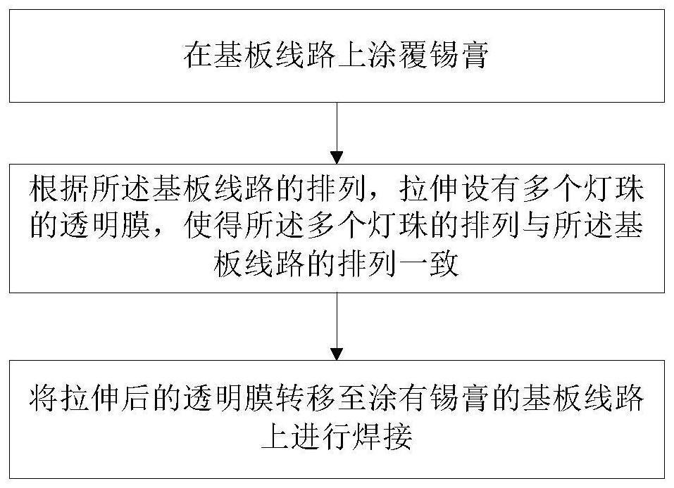
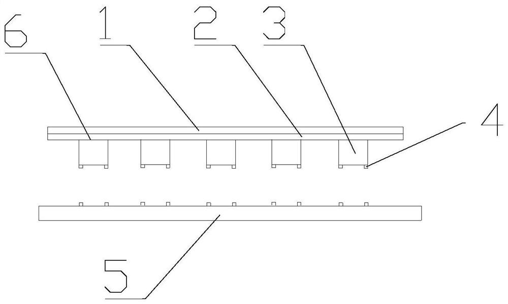
[0043] Please refer to figure 1 with figure 2 , a lamp bead welding method, comprising steps:
[0044] Coating solder paste on the circuit of the substrate 5;
[0045] The described coating of solder paste on the substrate 5 circuit is specifically:
[0046] Apply die-bonding solder paste on the circuit that needs to be soldered on the substrate 5;
[0047] Stretching the transparent film provided with a plurality of lamp beads 3 according to the arrangement of the circuits of the substrate 5, so that the arrangement of the plurality of lamp beads 3 is consistent with the arrangement of the circuits of the substrate 5;
[0048] According to the arrangement of the circuit of the substrate 5, stretching the transparent film provided with a plurality of lamp beads 3, so that the arrangement of the plurality of lamp beads 3 is consistent with the arrangement of the circuit of the substrate 5 is as follows:
[0049] Stretching the transparent film provided with a plurality of ...
Embodiment 2
[0060] This embodiment will further illustrate how the above lamp bead welding method of the present invention is realized in combination with specific application scenarios:
[0061] 1. Apply die-bonding solder paste on the circuit to be soldered on the substrate 5;
[0062] Specifically, a traditional coating machine can be used to coat the crystal-bonding solder paste, and different dosages of the crystal-bonding solder paste can be selected according to different models of the LED lamp bead 3;
[0063] 2. Stretch the transparent film provided with a plurality of LED lamp beads 3 in a crystal-expanding manner according to the arrangement of the circuits of the substrate 5, so that the arrangement of the plurality of LED lamp beads 3 is consistent with the arrangement of the circuits of the substrate 5;
[0064] Specifically, the range and shape of the stretched transparent film of the crystal expander can be set according to the arrangement of the basic lines, so as to ensu...
PUM
| Property | Measurement | Unit |
|---|---|---|
| thickness | aaaaa | aaaaa |
| thickness | aaaaa | aaaaa |
| Basis weight | aaaaa | aaaaa |
Abstract
Description
Claims
Application Information

