Active substrate and preparation method thereof

A technology of substrate and cover plate, applied in the field of active substrate and its preparation, can solve the problems of poor flatness of rewiring layer and inability to meet the requirements of sealed space, and achieve the effect of improving flatness, avoiding influence and avoiding pollution

Active Publication Date: 2019-04-09
SHANGHAI INST OF MICROSYSTEM & INFORMATION TECH CHINESE ACAD OF SCI +1
View PDF11 Cites 0 Cited by
  • Summary
  • Abstract
  • Description
  • Claims
  • Application Information

AI Technical Summary

Problems solved by technology

[0004] In view of the above-mentioned shortcomings of the prior art, the purpose of the present invention is to provide an active substrate and a preparation method thereof, which are used to solve the problems existing in the three-dimensional packaging technology in the prior art between the groove and the embedding period. Large gaps, resulting in poor flatness of the rewiring layer, and problems that cannot meet the needs of specific devices that require sealed spaces

Method used


Image

  • Active substrate and preparation method thereof
  • Active substrate and preparation method thereof
  • Active substrate and preparation method thereof

Examples


Embodiment 1

[0054] see figure 1 , the present embodiment provides a kind of preparation method of active substrate, and the preparation method of described active substrate comprises the following steps:

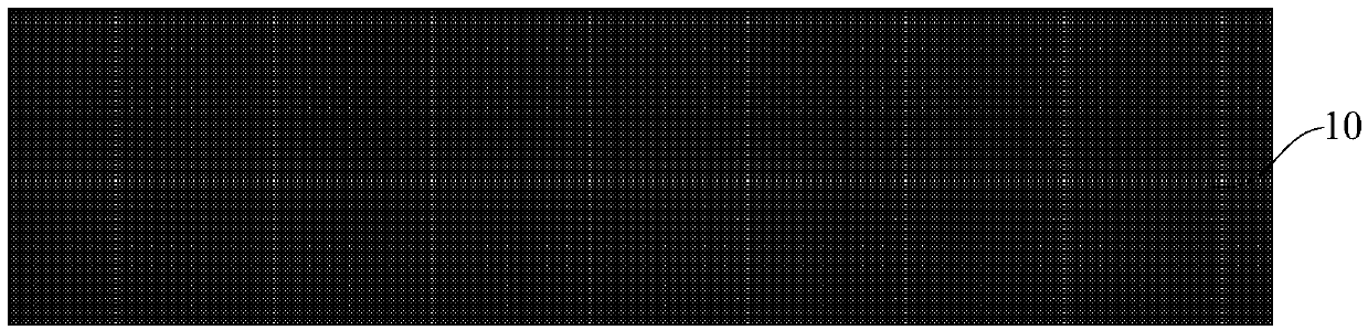
[0055] 1) providing a substrate;

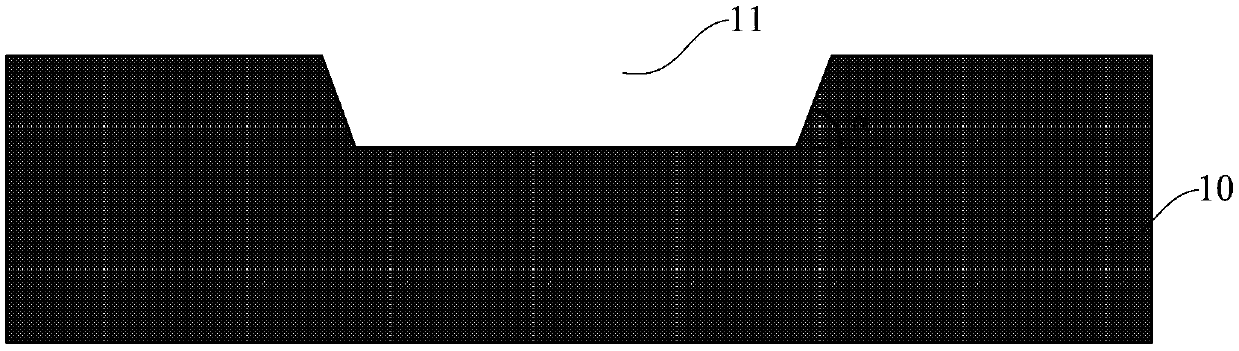
[0056] 2) forming grooves on the upper surface of the substrate;

[0057] 3) making a MEMS device at the bottom of the groove;

[0058] 4) making a metal interconnection structure on the substrate, the metal interconnection structure is electrically connected to the MEMS device, and extends from the MEMS device along the sidewall of the groove to the upper surface of the substrate, and cover the upper surface of the substrate;

[0059]5) Provide a cover plate, place the cover plate in the groove to form a sealed cavity between the cover plate and the bottom of the MEMS device, and seal the MEMS in the sealed cavity cavity;

[0060] 6) forming a first passivation layer on the substrate, the first passivation layer covering the metal interconnect st...

Embodiment 2

[0106] read on Figure 10 , the present invention also provides an active substrate, which includes: a substrate 10, a groove 11 is formed on the upper surface of the substrate 10; a MEMS device 12, the MEMS device 12 is located in the groove 11 Bottom; metal interconnection structure 13, described metal interconnection structure 13 is electrically connected with described MEMS device 12, and described metal interconnection structure 13 extends from described MEMS device 12 along the sidewall of described groove 11 to the described The upper surface of the substrate 10; the cover plate 14, the cover plate 14 is clamped inside the groove 11 to form a sealed cavity 111 between the cover plate 11 and the bottom of the MEMS device 12; The MEMS device 12 is sealed in the sealed cavity 111; a first passivation layer 15, the first passivation layer 15 is located on the upper surface of the substrate 10, and the first passivation layer 15 covers the The upper surface of the metal int...


PUM


Abstract

The invention provides an active substrate and a preparation method thereof. The active substrate comprises a substrate, in the upper surface of which a groove is formed; an MEMS device located at thebottom of the groove; a metal interconnection structure electrically connected with the MEMS device and extending from the MEMS device to the upper surface of the substrate along the side wall of thegroove; a cover plate clamped in the groove, so that a sealed cavity is formed between the cover plate and the bottom of the MEMS device; a first passivation layer located on the upper surface of thesubstrate; a redistribution layer on the first passivation layer; and a second passivation layer located on the upper surface of the first passivation layer. An opening is formed in the second passivation layer, and the part, exposed out of the opening, of the rewiring layer serves as a bonding pad. According to the active substrate provided by the invention, the groove and the cover plate are clamped and occluded to realize the installation of the cover plate, so that a traditional cover plate bonding process is omitted. According to the active substrate disclosed by the invention, the MEMSdevice is sealed in the sealed cavity by adopting the cover plate, so that the influence of particles, moisture and the like on the MEMS device is avoided, and the reliability of the MEMS device is improved.

Description

technical field [0001] The invention belongs to the technical field of three-dimensional packaging, and in particular relates to an active substrate and a preparation method thereof. Background technique [0002] Three-dimensional (3D) packaging technology is a high-density packaging technology developed in space on the basis of two-dimensional packaging in the X-Y plane. The pursuit of lighter, thinner, and smaller products in communications, computers, automotive electronics, aerospace, and other consumer products has driven the development of microelectronic packaging toward high-density three-dimensional (3D) packaging. Three-dimensional (3D) packaging not only improves the packaging density, reduces the packaging cost, reduces the length of the interconnection wires between each chip, and improves the operating speed of the device, but also realizes the function of the device through chip stacking or package stacking. increase. Three-dimensional (3D) packaging has unp...

Claims


Application Information

Patent Timeline
Patent Type & Authority Applications(China)
IPC IPC(8): B81B7/00B81C1/00
CPCB81B7/0032B81B7/007B81B7/0074B81C1/00261B81C1/00269B81C1/00301
Inventor 徐高卫胡正高盖蔚吴亚明
Owner SHANGHAI INST OF MICROSYSTEM & INFORMATION TECH CHINESE ACAD OF SCI
Why Eureka
Try Eureka