A packaging structure of an image sensor and its packaging process

An image sensor and packaging structure technology, which is applied to electric solid-state devices, semiconductor devices, radiation control devices, etc., can solve the problems of inability to meet the packaging requirements of image sensors, high packaging cost, and high height, so as to save the wire bonding process. , The effect of reducing packaging costs and shortening the process flow

Active Publication Date: 2017-12-08
JACAL ELECTRONICS WUXI
View PDF3 Cites 0 Cited by
  • Summary
  • Abstract
  • Description
  • Claims
  • Application Information

AI Technical Summary

Problems solved by technology

[0002] Existing image sensors usually install the chip in the cavity of the base (such as CLCC ceramic base, PLCC organic base), interconnect the chip and the base with gold wire or aluminum wire, and then use glass plate light window to bond and seal ; Then there is the wafer-level packaging that uses through-silicon via technology (TSV) for vertical conduction. The former has the disadvantages of large height and size, while the latter has shortcomings such as large investment and high packaging cost, which cannot meet the requirements of ultra-thin and ultra-small size. Sensor Packaging Requirements

Method used


Image

  • A packaging structure of an image sensor and its packaging process
  • A packaging structure of an image sensor and its packaging process
  • A packaging structure of an image sensor and its packaging process

Examples


Embodiment

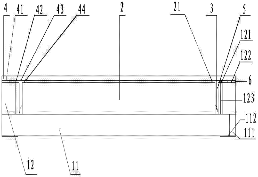
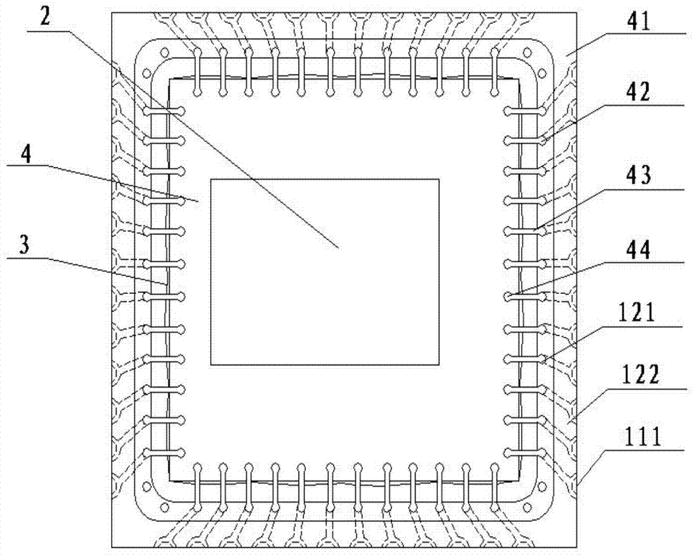
[0052] Embodiment: A 0.70mm pitch PLCC48 packaging structure and packaging process for an ultra-thin image sensor with a size of 10mm×10mm×0.85mm, including the following steps:

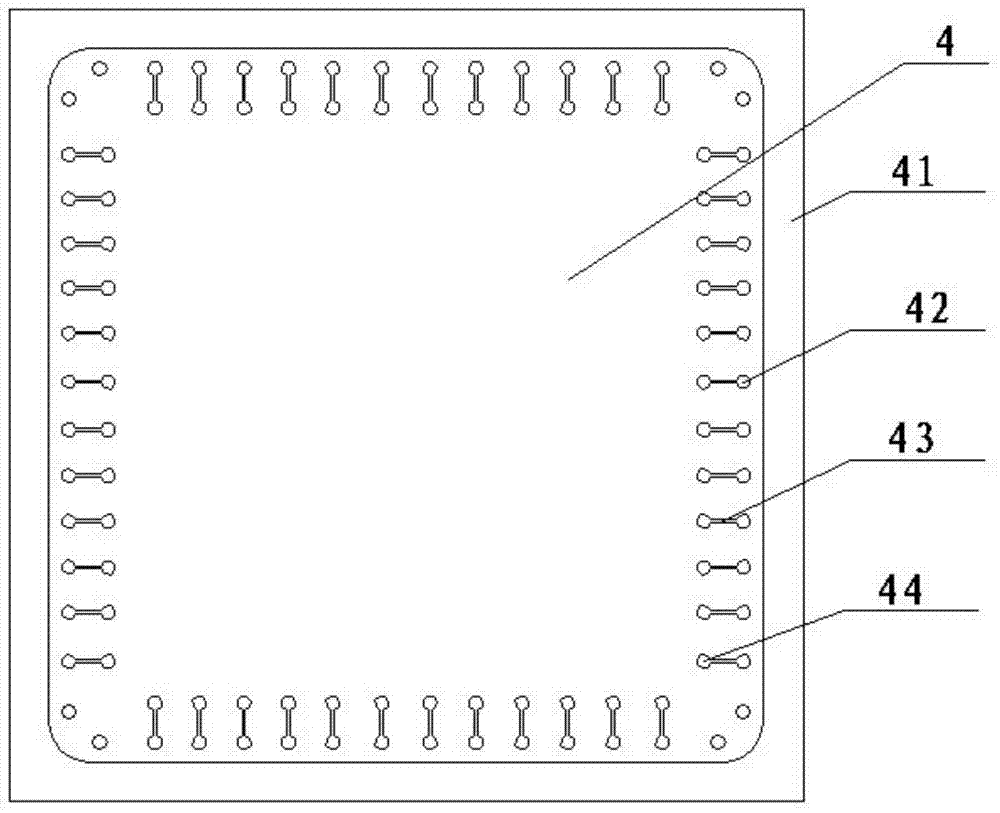
[0053] Firstly, the SCHOTT AF32 series eco aluminoborosilicate glass with a thickness of 0.10mm is photolithographically etched and evaporated on one side of the film glass through a mask to prepare a sealing ring 41, an outer pad 42, an interconnection line 43, and an inner pad 44 , the metal layer is a Cr-Ni-Ag layer with a thickness of 600 angstroms to 2000 angstroms, 2000 angstroms to 7000 angstroms, and 500 angstroms to 1000 angstroms; finally, it is cut into a thin film glass window 4 of 9.8mm×9.8mm×0.05mm, such as figure 1 ;

[0054] Secondly, use FR4 material and copper foil to make pad 121 with support part, support part sealing ring 122, PLCC48 substrate 1 of 10mm×10mm×0.70mm with buried hole 123, base outer pad 112, semicircular through hole 111, thermally spray SnAg0.3Cu0. 7 Solder laye...


PUM


Abstract

The invention discloses a packaging structure of an image sensor. The packaging structure of the image sensor comprises a substrate; the substrate comprises a base part; the rim part of the upper surface of the base part is extended upward to form an enclosed type support part; the upper surface of the base part in the cavity formed by the support part and the base part is fixedly provided with an image sensor chip in an adhesion manner through an adhesion layer; a sealing connection ring, an external welding plate, an interconnection line and an inner welding plate are successively manufactured on the rim of the bottom end of the film glass optical window through optical etching, evaporation or sputtering from the outside to the inside; the upper end surface of the support part is provided with a support part welding plate cooperating with an external welding plate on the side close to the image sensor; the support part upper end surface of the external side of the support part welding plate is provided with a support part sealing connection ring cooperating with the sealing connection ring; a plurality of semicircular through holes are arranged on the circumferential rim of the base part at equal interval, wherein the breaches of the semicircular through holes face outward and the lower end of the semicircular through hole is communicated with the lower end surface of the base part; and the bottom end surface of the base part is provided with a base part external welding plate.

Description

technical field [0001] The invention relates to the technical field of microelectronic packaging, in particular to a packaging structure of an image sensor and a packaging process thereof. Background technique [0002] Existing image sensors usually install the chip in the cavity of the base (such as CLCC ceramic base, PLCC organic base), interconnect the chip and the base with gold wire or aluminum wire, and then use glass plate light window to bond and seal ; Then there is the wafer-level packaging that uses through-silicon via technology (TSV) for vertical conduction. The former has the disadvantages of large height and size, while the latter has shortcomings such as large investment and high packaging cost, which cannot meet the requirements of ultra-thin and ultra-small size. Sensor packaging requirements. [0003] Aiming at the problems in the related technologies, no effective solution has been proposed yet. Contents of the invention [0004] The object of the pre...

Claims


Application Information

Patent Timeline
Patent Type & Authority Patents(China)
IPC IPC(8): H01L27/146
CPCH01L27/14636H01L27/1469
Inventor 王国建李保云
Owner JACAL ELECTRONICS WUXI
Why Eureka
Try Eureka