Defect detection system and defect detection method

A defect detection and defect technology, which is applied in the direction of optical test defect/defect, measurement device, material analysis through optical means, etc., can solve problems such as poor performance, and achieve the effect of improving performance and stabilizing product yield

Inactive Publication Date: 2019-04-09
HUAIAN IMAGING DEVICE MFGR CORP
View PDF8 Cites 7 Cited by
  • Summary
  • Abstract
  • Description
  • Claims
  • Application Information

AI Technical Summary

Problems solved by technology

[0004] However, existing systems for wafer surface defect detection perform poorly

Method used


Image

  • Defect detection system and defect detection method
  • Defect detection system and defect detection method
  • Defect detection system and defect detection method

Examples


Embodiment Construction

[0023] As mentioned in the background, the performance of existing systems for wafer surface defect detection is poor.

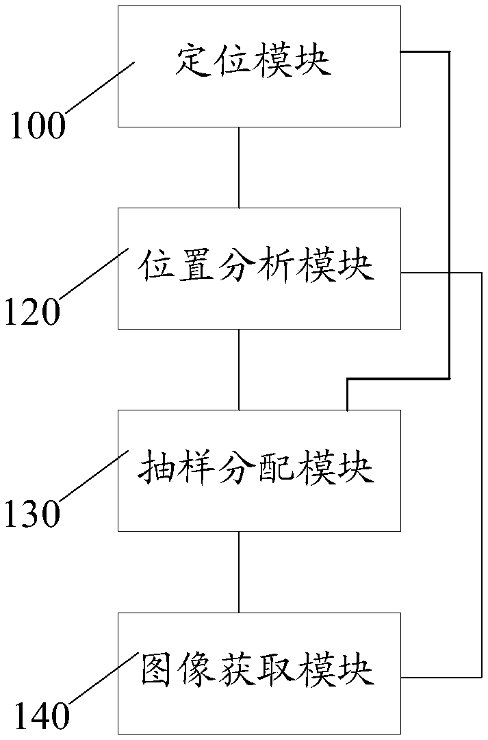
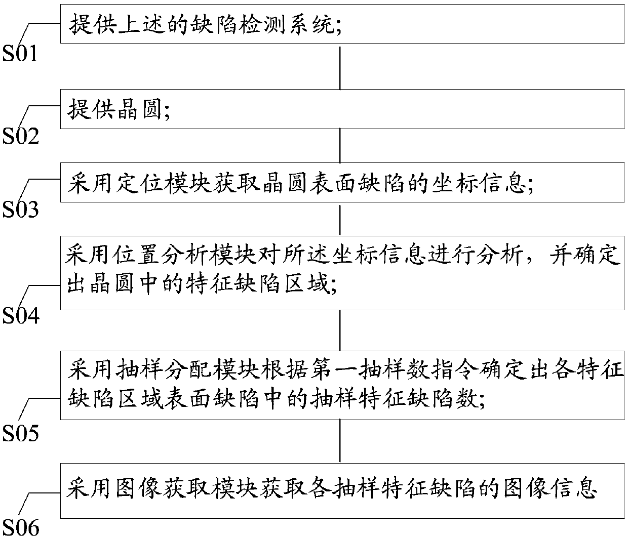
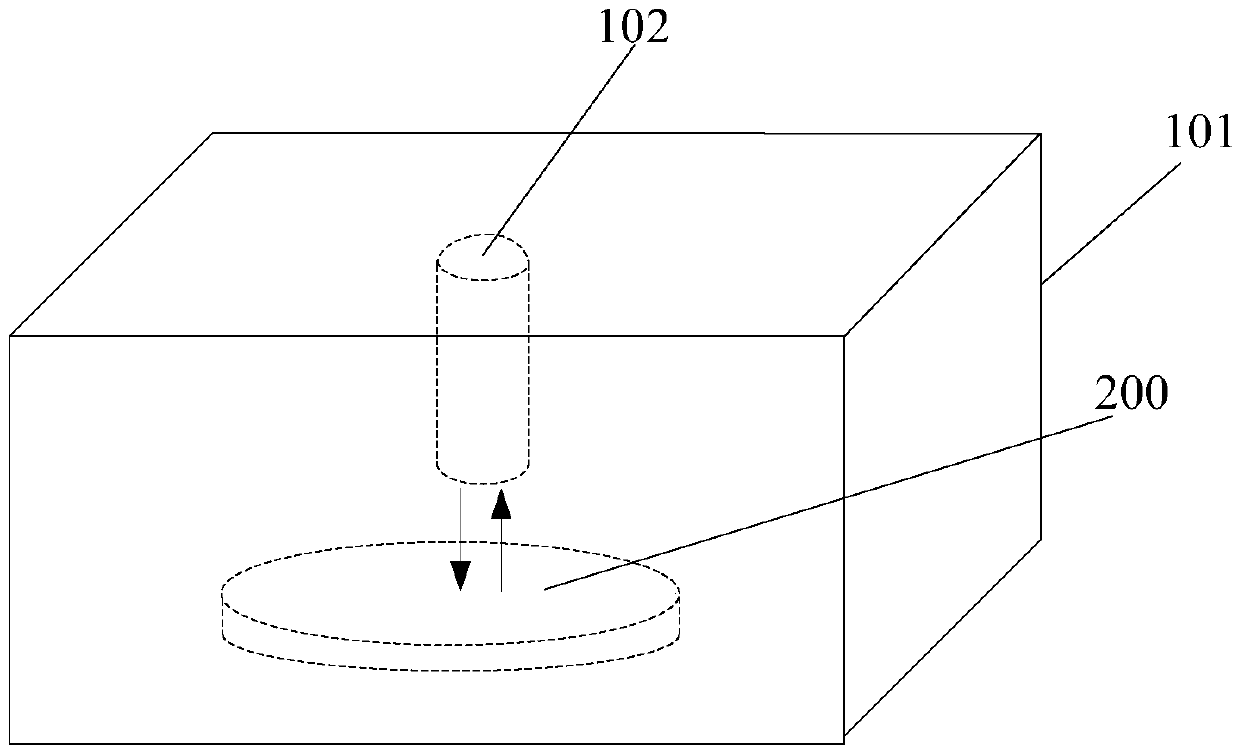
[0024] A defect detection method, comprising: providing a bright-field and dark-field scanning machine; providing an image acquisition module, the image acquisition module including a random sampling module and an image acquisition module; using the bright-field and dark-field scanning machine to obtain the surface defects of the wafer Coordinate information; the random sampling module is used to sample the coordinate information of defect points; the image acquisition module performs image acquisition on the extracted defect points. Then analyze the defect point according to the image information of the defect point.

[0025] When the distribution of defect points in certain areas of the wafer is relatively special, it is necessary to analyze the defect points on the surface of the special area. However, due to the randomness of the defect point sampling b...


PUM


Abstract

The invention discloses a defect detection system and a defect detection method. The system comprises a positioning module suitable to acquire coordinate information of surface defects of a wafer, a position analysis module suitable to analyze the coordinate information and determine feature defect regions in the wafer, a sampling distribution module suitable to determine sampling feature defectsin the surface defects of the feature defect regions according to a first sampling quantity instruction, and an image acquisition module suitable to acquire image information of the sampling feature defects. The performance of the defect detection system is improved.

Description

technical field [0001] The invention relates to the field of semiconductor testing, in particular to a defect detection system and a defect detection method. Background technique [0002] After the wafer has gone through the process, the surface of the wafer needs to be inspected to determine whether the process is proceeding normally by inspecting the wafer. Defect detection on the wafer surface is an important content. [0003] Usually, there will be a certain number of defects on the surface of the wafer, and the defects on the surface of the wafer need to be analyzed in order to detect abnormalities in time and improve the process. [0004] However, existing systems for wafer surface defect detection perform poorly. Contents of the invention [0005] The problem solved by the present invention is to provide a defect detection system and a defect detection method to improve the performance of the defect detection system. [0006] In order to solve the above problems,...

Claims


Application Information

Patent Timeline
Patent Type & Authority Applications(China)
IPC IPC(8): G01N21/95
CPCG01N21/9501
Inventor 许平康方桂芹黄仁德
Owner HUAIAN IMAGING DEVICE MFGR CORP
Why Eureka
Try Eureka