A mems scanning mirror

A scanning mirror and mirror surface technology, applied in the field of MEMS scanning mirrors, can solve the problems of increasing circuit complexity, increasing film deposition difficulty, piezoelectric film breakdown, etc., and achieving good device driving performance, simple structure, and high device reliability. Effect

Active Publication Date: 2022-01-25
SHENZHEN GRADUATE SCHOOL TSINGHUA UNIV
View PDF6 Cites 0 Cited by
  • Summary
  • Abstract
  • Description
  • Claims
  • Application Information

AI Technical Summary

Problems solved by technology

However, a large driving voltage is easy to break down the piezoelectric film, and at the same time brings many additional effects, increasing the complexity of the circuit
Large driving voltage also puts forward higher requirements on the quality of the piezoelectric film, increasing the difficulty of film deposition

Method used


Image

  • A mems scanning mirror
  • A mems scanning mirror

Examples


Embodiment Construction

[0022] Embodiments of the present invention will be described in detail below. It should be emphasized that the following description is only exemplary and not intended to limit the scope of the invention and its application.

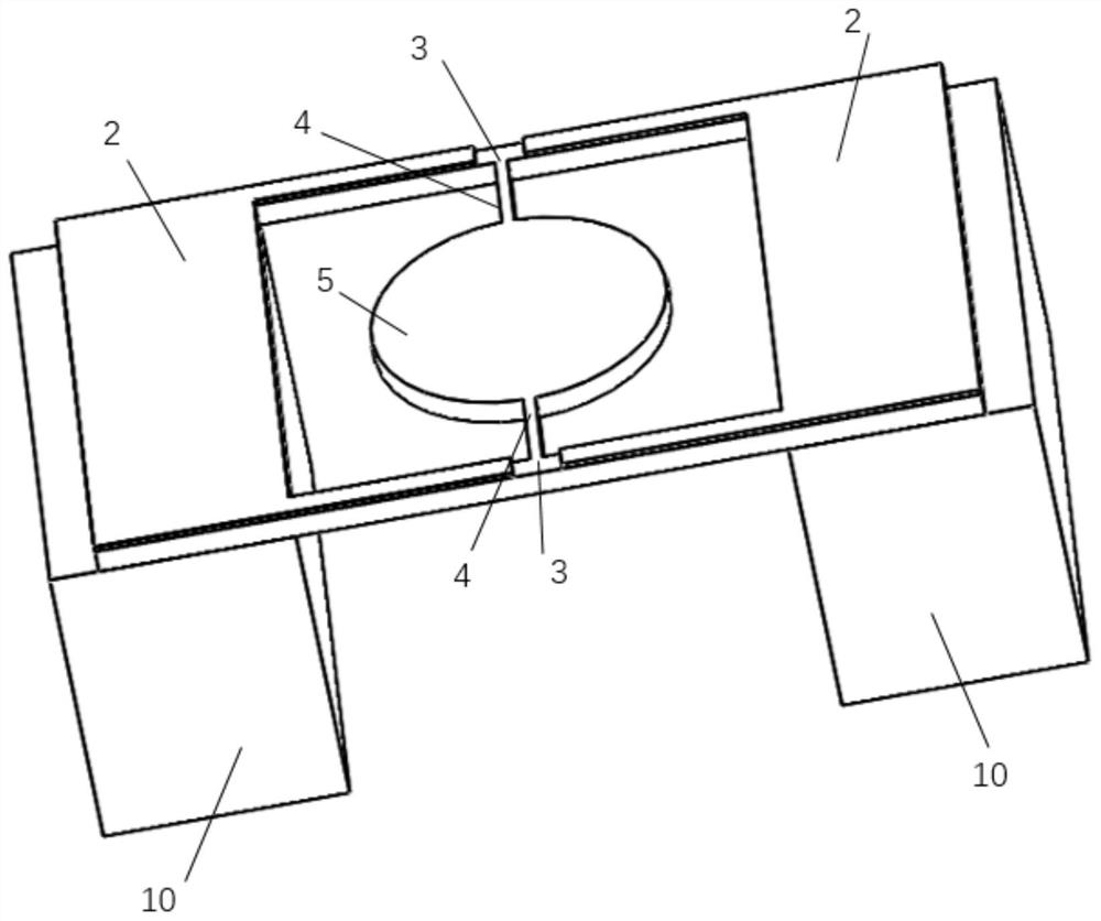
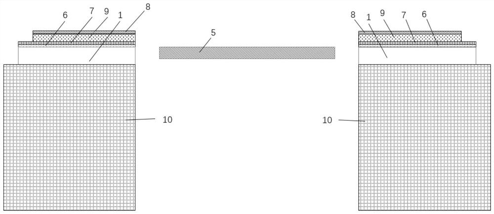
[0023] refer to figure 1 and figure 2 , in one embodiment, a MEMS scanning mirror includes two piezoelectric ceramic blocks 10, two piezoelectric driving arms 2, two beams 3, two torsion beams 4 and a mirror surface 5, the two There is a distance between the piezoelectric ceramic blocks 10, the two piezoelectric driving arms 2 are respectively arranged on the two piezoelectric ceramic blocks 10, and the two beams 3 are connected in parallel to the two piezoelectric driving arms. Between the arms 2, the two torsion beams 4 and the mirror surface 5 are connected in series between the two beams 3, and the mirror surface 5 is connected between the two torsion beams 4; The voltages applied to the two piezoelectric driving arms 2 are opposite, so that the...


PUM

PropertyMeasurementUnit
lengthaaaaaaaaaa
widthaaaaaaaaaa
thicknessaaaaaaaaaa

Abstract

A MEMS scanning mirror, including two piezoelectric ceramic blocks, two piezoelectric driving arms, two beams, two torsion beams and a reflector surface, there is a separation distance between the two piezoelectric ceramic blocks, and the two piezoelectric driving arms They are respectively arranged on two piezoelectric ceramic blocks, two beams are connected in parallel between two piezoelectric driving arms, two torsion beams and reflective mirrors are connected in series between the two beams, and the reflective mirrors are connected to two torsion Between the beams; the voltages applied to the two piezoelectric driving arms are opposite, so that the two piezoelectric driving arms bend in opposite directions, and the mirror surface is deflected; the voltages applied to the two piezoelectric ceramic blocks are opposite, so that the two piezoelectric The deformation of the ceramic block in the opposite direction to the direction perpendicular to the mirror surface drives the deflection of the mirror surface, and superimposes with the deflection angle of the mirror surface caused by the piezoelectric drive arm to amplify the deflection angle of the mirror surface. The scanning mirror can realize a large deflection angle, and has the advantages of small size, high reliability, simple structure and manufacturing process.

Description

technical field [0001] The invention relates to the field of micro-opto-electromechanical devices, in particular to a MEMS scanning mirror. Background technique [0002] As the core component of optical scanning, optical scanning mirror plays an important role in projection display, optical imaging and other systems. Compared with traditional optical scanning mirrors, MEMS scanning mirrors not only have the low cost and easy mass production common to MEMS devices, but also have better optical and mechanical properties, especially in terms of dynamic response and power consumption. . [0003] The actuators in MEMS optical devices and systems must have the characteristics of small size, good driving performance, accurate work, low power consumption, high reliability, and easy manufacturing. [0004] At present, MEMS scanning mirrors have various drive methods such as electrostatic drive, electromagnetic drive, piezoelectric drive, and thermal drive. The response of the ther...

Claims


Application Information

Patent Timeline
Patent Type & Authority Patents(China)
IPC IPC(8): G02B26/08G02B26/10
CPCG02B26/0858G02B26/105
Inventor 董瑛李思萦王晓浩
Owner SHENZHEN GRADUATE SCHOOL TSINGHUA UNIV
Why Eureka
Try Eureka