Optimization method of molecular beam epitaxy growth AlInAsSb superlattice material

A molecular beam epitaxy and optimization method technology, applied in the field of semiconductor materials, can solve the problems of poor uniformity of large areas of materials, complex device manufacturing processes, and device application limitations

Active Publication Date: 2019-04-12
YUNNAN NORMAL UNIV
View PDF8 Cites 6 Cited by
  • Summary
  • Abstract
  • Description
  • Claims
  • Application Information

AI Technical Summary

Problems solved by technology

However, the growth process of this infrared detector material requires high requirements, and a complex device manufacturing process is required. The large-area uniformity of the material is poor, which greatly limits the application of this type of device.

Method used


Image

  • Optimization method of molecular beam epitaxy growth AlInAsSb superlattice material
  • Optimization method of molecular beam epitaxy growth AlInAsSb superlattice material
  • Optimization method of molecular beam epitaxy growth AlInAsSb superlattice material

Examples


Embodiment Construction

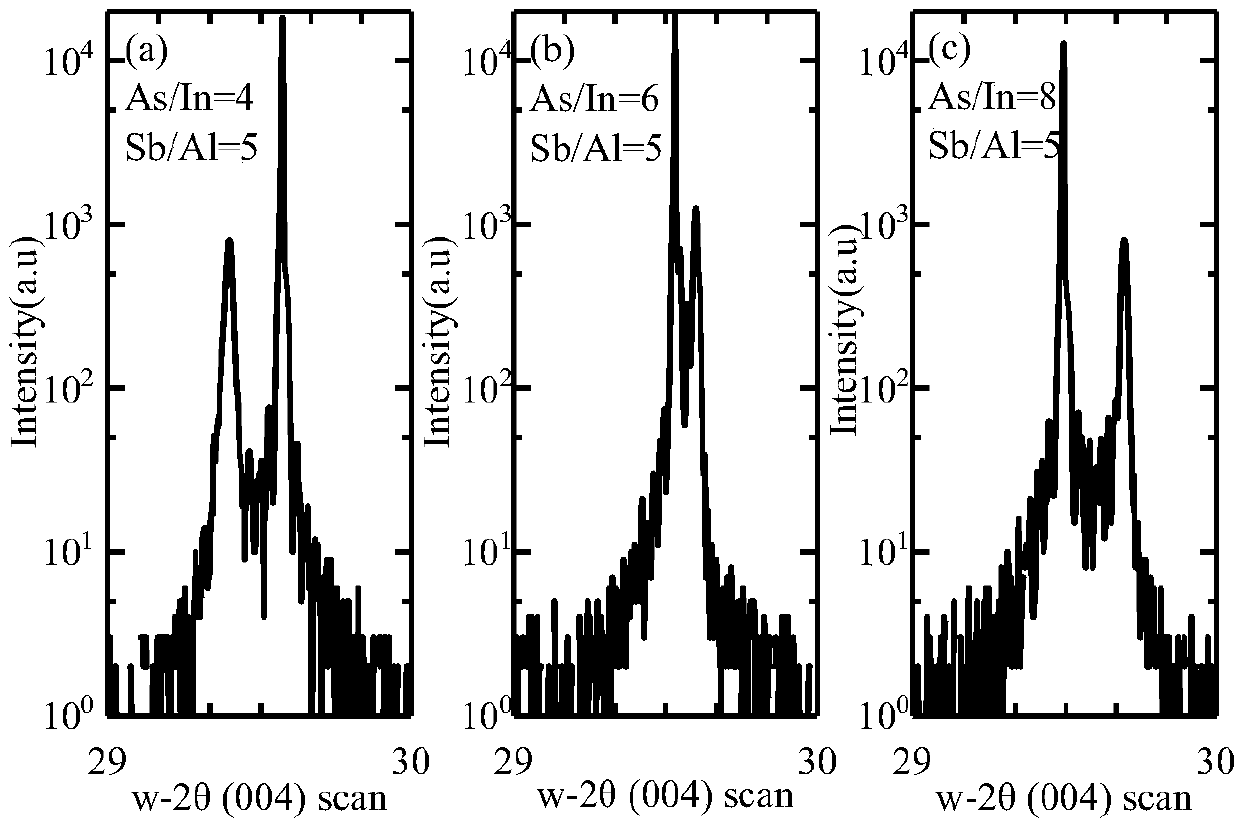
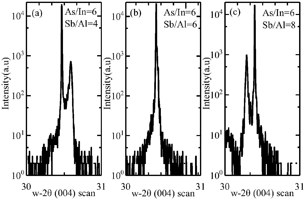
[0035] In this embodiment, an optimized growth method of a short-wavelength AlInAsSb superlattice material is provided. The structure used in the material optimization growth method is as follows from bottom to top: GaSb substrate, 200nm thick GaSb buffer layer, 30nm AlSb barrier layer, 40 periods of AlInAsSb superlattice, 30nm AlSb barrier layer and 20nm GaSb capping layer. Among them, the AlSb layer above and below the superlattice is used to limit the movement of carriers for better PL spectrum testing. The method adopts the alloy technology to prepare the AlInAsSb superlattice material, and the shutter sequence is as follows: AlSb, AlAs, AlSb, Sb, In, InAs, In, Sb (the interface sequence is an optimized sequence). The optimization method of the present invention comprises the following specific steps:

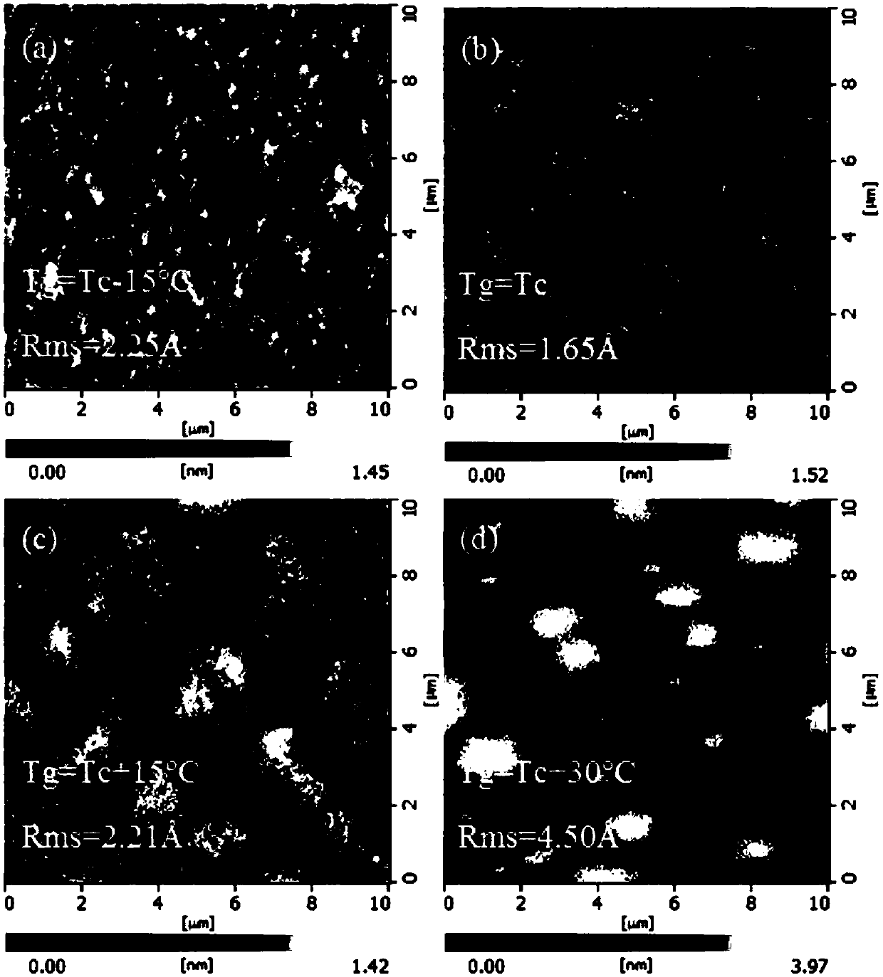
[0036] (1) Substrate pre-degassing: put a 2-inch double-sided polished GaSb substrate into the intro chamber, and wait until the vacuum degree is reduced to 1.6×10 -6 A...


PUM


Abstract

The invention discloses an optimization method of a molecular beam epitaxy growth short wave infrared AlInAsSb superlattice; the method comprises the following steps of determining the source furnacetemperature and the corresponding beam current values of three-group elements in AlInAsSb, and the corresponding beam flow values of five-group elements and the reference temperature Tc of the epitaxial growth of the molecular beams, and defining the beam-flow value ratios of the five-group elements to the three-group elements as Sb/Al and As/In; setting the value of the Sb/Al to be a fixed valueA, and setting the value of the As/In as a variable value x, and analyzing and determining the optimal value xi of the As/In by comparing the Xrd graph of different x values; similarly, setting the value of the As/In to be the optimal value xi, and setting the value of the Sb/Al as a variable value y, and analyzing and determining the optimal value yi of the Sb/Al by comparing the Xrd graph of different y values; and adjusting the growth temperature of the AlInAsSb superlattice on a GaSb substrate by using a step length of 15 DEG C according to the reference temperature Tc, and determining theoptimal growth temperature according to the surface roughness of the AFM graph. By means of the optimization method, the AlInAsSb material with high material quality can be obtained, and the method is simple and efficient.

Description

technical field [0001] The invention discloses an optimization method for growing a short-wave infrared detection material AlInAsSb superlattice by using molecular beam epitaxy technology, belonging to the field of semiconductor materials. Background technique [0002] Today, short-wave infrared (SWIR) detectors in the 1-3 micron band have important application prospects in military and civilian fields, including secure communications, astronomical observations, gas analysis, and earth sciences. Cameras equipped with SWIR imaging can obtain higher resolution images than traditional visible light cameras. In addition, imaging in this wavelength range allows for passive and active imaging. Therefore, it has very important application value in military and civilian fields. So far, many material systems, such as mercury cadmium telluride HgCdTe (MCT) and indium gallium arsenide In x Ga 1-x As, a lot has been addressed in this band. They made the cutoff wavelength of the mat...

Claims


Application Information

Patent Timeline
Patent Type & Authority Applications(China)
IPC IPC(8): H01L21/02H01L21/67H01L31/18H01L31/0304H01L31/0352
CPCH01L21/02398H01L21/02546H01L21/02549H01L21/02631H01L21/67253H01L31/03046H01L31/035236H01L31/1844Y02P70/50
Inventor 郝瑞亭常发冉郭杰李勇刘欣星顾康刘斌王璐
Owner YUNNAN NORMAL UNIV
Why Eureka
Try Eureka