A kind of vcsel chip and manufacturing method thereof

A manufacturing method and chip technology, applied to laser parts, semiconductor lasers, electrical components, etc., can solve the problem of low power of VCSEL chips, and achieve the effects of improving surface morphology, improving quality, and low threshold current

Active Publication Date: 2020-06-26
YANGZHOU CHANGELIGHT
View PDF6 Cites 0 Cited by
  • Summary
  • Abstract
  • Description
  • Claims
  • Application Information

AI Technical Summary

Problems solved by technology

[0003] In view of this, the present invention provides a kind of VCSEL chip and manufacturing method thereof, to solve the problem that the power of existing VCSEL chip is still low

Method used


Image

  • A kind of vcsel chip and manufacturing method thereof
  • A kind of vcsel chip and manufacturing method thereof
  • A kind of vcsel chip and manufacturing method thereof

Examples


Embodiment Construction

[0038] The above is the core idea of ​​the present invention. In order to make the above-mentioned purposes, features and advantages of the present invention more obvious and easy to understand, the technical solutions in the embodiments of the present invention will be clearly and completely described below in conjunction with the accompanying drawings in the embodiments of the present invention Description, obviously, the described embodiments are only a part of the embodiments of the present invention, rather than all the embodiments. Based on the embodiments of the present invention, all other embodiments obtained by persons of ordinary skill in the art without making creative efforts belong to the protection scope of the present invention.

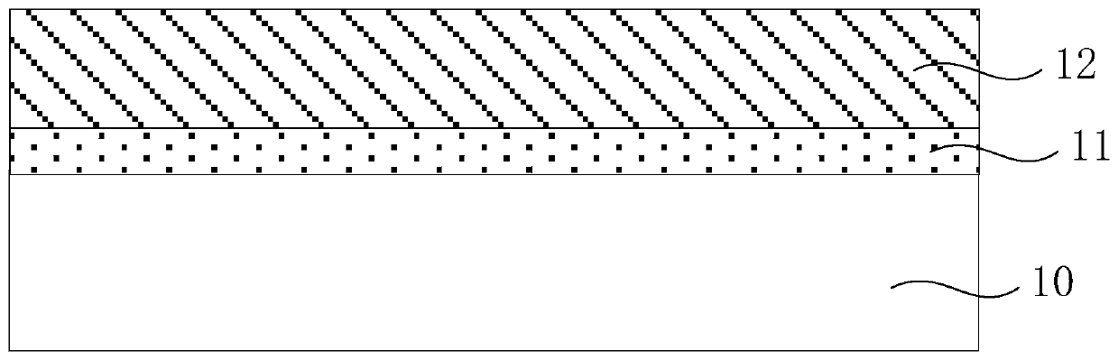
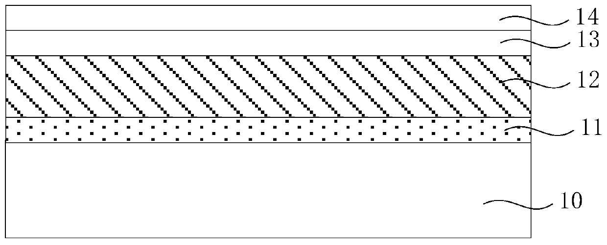
[0039] The embodiment of the present invention provides a kind of manufacturing method of VCSEL chip, such as figure 1 shown, including:

[0040] S101: Provide a sample, the sample includes a substrate and an epitaxial structure laye...


PUM


Abstract

The invention provides a VCSEL chip and a manufacturing method thereof. The method comprises the following steps of providing a sample, wherein the sample comprises a substrate and an epitaxial structure layer located on the surface of the substrate, and the epitaxial structure layer comprises a first semiconductor layer, an MQW layer, a second semiconductor layer and a first GaAs buffer layer; performing a plurality of stages of baking on the sample, and in at least one stage of the middle, performing baking on the sample in an As source gas; and growing a second GaAs buffer layer on the surface of the epitaxial structure layer by adopting an intermittent growth method. The sample is baked for multiple stages, so that impurities, glue and the like on the surface of the sample can be eliminated, thereby improving the quality of a subsequently formed film layer; the second GaAs buffer layer is grown by adopting the intermittent growth method, so that the second GaAs buffer layer can have a smooth surface, and then the quality of the subsequently formed film layer can be improved, and therefore the VCSEL chip can have a relatively low threshold current, relatively high gain and higher power.

Description

technical field [0001] The invention relates to the field of optoelectronic technology, more specifically, to a VCSEL chip and a manufacturing method thereof. Background technique [0002] VCSEL (Vertical-Cavity Surface-Emitting Laser) chip has the advantages of small size, circular output spot, single longitudinal mode output, small threshold current, low price and easy integration into a large-area array. It is widely used in optical communication, optical interconnection and optical storage and other fields. However, the power of existing VCSEL chips is still low. Contents of the invention [0003] In view of this, the present invention provides a VCSEL chip and a manufacturing method thereof, so as to solve the problem that the power of the existing VCSEL chip is still low. [0004] To achieve the above object, the present invention provides the following technical solutions: [0005] A method for making a VCSEL chip, comprising: [0006] providing a sample, the sa...

Claims


Application Information

Patent Timeline
Patent Type & Authority Patents(China)
IPC IPC(8): H01S5/343H01S5/183
CPCH01S5/183H01S5/3432
Inventor 田宇韩效亚吴真龙杜石磊
Owner YANGZHOU CHANGELIGHT
Why Eureka
Try Eureka