Check patentability & draft patents in minutes with Patsnap Eureka AI!

Band-gap reference voltage circuit

A reference voltage and reference voltage output technology, applied in the direction of adjusting electrical variables, control/regulation systems, instruments, etc., can solve the problem of low power supply suppression, achieve the effect of reducing quantity and reducing manufacturing cost

Active Publication Date: 2019-04-16
SHANGHAI BEILING
View PDF5 Cites 0 Cited by
  • Summary
  • Abstract
  • Description
  • Claims
  • Application Information

AI Technical Summary

Problems solved by technology

[0007] The technical problem to be solved by the present invention is to provide a bandgap reference voltage circuit in order to overcome the defect that the power supply rejection ratio of the bandgap reference voltage circuit in the prior art is relatively low

Method used


Image

  • Band-gap reference voltage circuit
  • Band-gap reference voltage circuit
  • Band-gap reference voltage circuit

Examples


Embodiment 1

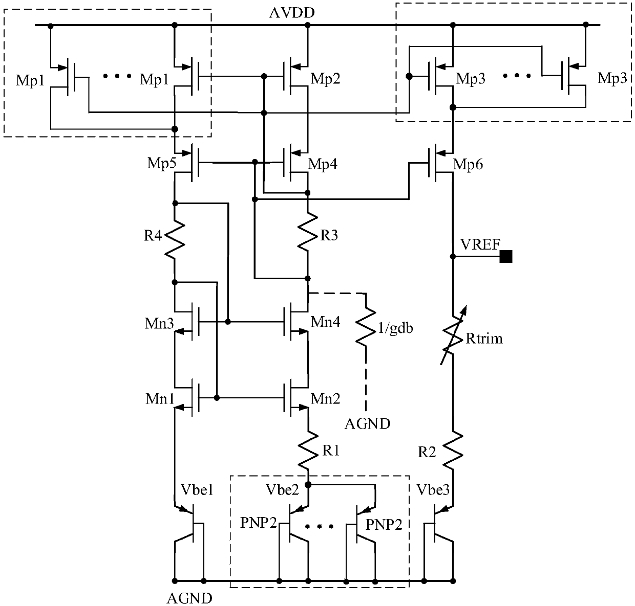
[0036] This embodiment provides a bandgap reference voltage circuit, referring to image 3, the bandgap reference voltage circuit includes: a reference voltage output terminal VREF, a first PMOS transistor Mp1, a second PMOS transistor Mp2, a third PMOS transistor Mp3, a fourth PMOS transistor Mp4, a fifth PMOS transistor Mp5, and a sixth PMOS transistor Mp6 , the first NMOS transistor Mn1, the second NMOS transistor Mn2, the third NMOS transistor Mn3, the fourth NMOS transistor Mn4, the first PNP transistor PNP1, the second PNP transistor PNP2, the third PNP transistor PNP3, the first resistor R1, the second Resistor R2, third resistor R3, fourth resistor R4, adjustable resistor Rtrim.

[0037] The number of the first PMOS transistors Mp1 is n, and n is a positive integer. The sources of the transistor Mp5 are electrically connected, and the gates of the n first PMOS transistors Mp1 are electrically connected to the gates of the second PMOS transistors Mp2.

[0038] The num...

Embodiment 2

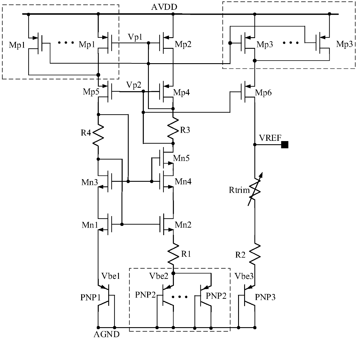
[0055] This embodiment provides a bandgap reference voltage circuit, referring to Image 6 , the bandgap reference voltage circuit includes: a reference voltage output terminal VREF, a first PMOS transistor Mp1, a second PMOS transistor Mp2, a third PMOS transistor Mp3, a fourth PMOS transistor Mp4, a fifth PMOS transistor Mp5, and a sixth PMOS transistor Mp6 , the first NMOS transistor Mn1, the second NMOS transistor Mn2, the optimized third NMOS transistor Mn31, the optimized fourth NMOS transistor Mn41, the first PNP transistor PNP1, the second PNP transistor PNP2, the third PNP transistor PNP3, the first resistor R1, the second resistor R2, the third resistor R3, the fourth resistor R4, and the adjustable resistor Rtrim.

[0056] The number of the first PMOS transistors Mp1 is n, and n is a positive integer. The sources of the transistor Mp5 are electrically connected, and the gates of the n first PMOS transistors Mp1 are electrically connected to the gates of the second ...


PUM


Abstract

The invention discloses a band-gap reference voltage circuit comprising a first PMOS transistor, a second PMOS transistor, a third PMOS transistor, a fourth PMOS transistor, a fifth PMOS transistor, asixth PMOS transistor, a first NMOS transistor, a second NMOS transistor, a third NMOS transistor, a fourth NMOS transistor, a first PNP triode, a second PNP triode, a third PNP triode, a first resistor, a second resistor, a third resistor, a fourth resistor and an adjustable resistor. The fifth NMOS transistor is a zero threshold voltage MOS transistor, the drain electrode of the fifth NMOS transistor is electrically connected to the other end of the third resistor, the grid electrode of the fifth NMOS transistor is electrically connected to the grid electrode of the fourth NMOS transistor,and the source electrode of the fifth NMOS transistor is electrically connected with the drain electrode of the fourth NMOS transistor. The band-gap reference voltage circuit solves the problem that the capacity of the band-gap reference voltage circuit in suppressing the power source change is decreased when the power supply voltage is high, and the manufacturing cost is reduced.

Description

technical field [0001] The invention belongs to the technical field of analog integrated circuits, in particular to a bandgap reference voltage circuit. Background technique [0002] With the development of integrated circuit technology, System-On-Chip (SOC) has been widely used, and is developing in the direction of low power consumption, high speed, and small area. A great feature. As the core module of the analog circuit, the bandgap reference voltage circuit provides each module with a reference voltage that does not change with voltage, temperature, and manufacturing process as much as possible. Traditionally, the bandgap reference voltage is generated by utilizing the positive temperature coefficient of the bipolar triode emitter junction under different current density biases combined with the negative temperature coefficient of the emitter junction itself. figure 1 Shows the structure of a bandgap reference voltage circuit, NMOS (N-type metal-oxide-semiconductor) t...

Claims


Application Information

Patent Timeline
IPC IPC(8): G05F1/567
CPCG05F1/567
Inventor 何伟伟罗赛张煜彬张巍陈宁郑晓燕袁文师李鹏
Owner SHANGHAI BEILING
Features
  • R&D
  • Intellectual Property
  • Life Sciences
  • Materials
  • Tech Scout
  • Unparalleled Data Quality
  • Higher Quality Content
  • 60% Fewer Hallucinations
Learn More