Array substrate, display panel and film crack detection method

A technology for crack detection and array substrates, which is applied in semiconductor/solid-state device testing/measurement, semiconductor/solid-state device components, semiconductor devices, etc. The effect of loss and improvement of accuracy

Inactive Publication Date: 2019-04-16
KUNSHAN GO VISIONOX OPTO ELECTRONICS CO LTD
View PDF6 Cites 11 Cited by
  • Summary
  • Abstract
  • Description
  • Claims
  • Application Information

AI Technical Summary

Problems solved by technology

[0004] Embodiments of the present invention provide an array substrate, a display panel, and a film layer crack detection method to solve the problem that cracks in the circuit film layer of the array substrate cannot be detected immediately

Method used


Image

  • Array substrate, display panel and film crack detection method
  • Array substrate, display panel and film crack detection method
  • Array substrate, display panel and film crack detection method

Examples


Embodiment Construction

[0027] The following will clearly and completely describe the technical solutions in the embodiments of the present invention with reference to the accompanying drawings in the embodiments of the present invention. Obviously, the described embodiments are some of the embodiments of the present invention, but not all of them. Based on the embodiments of the present invention, all other embodiments obtained by persons of ordinary skill in the art without creative efforts fall within the protection scope of the present invention.

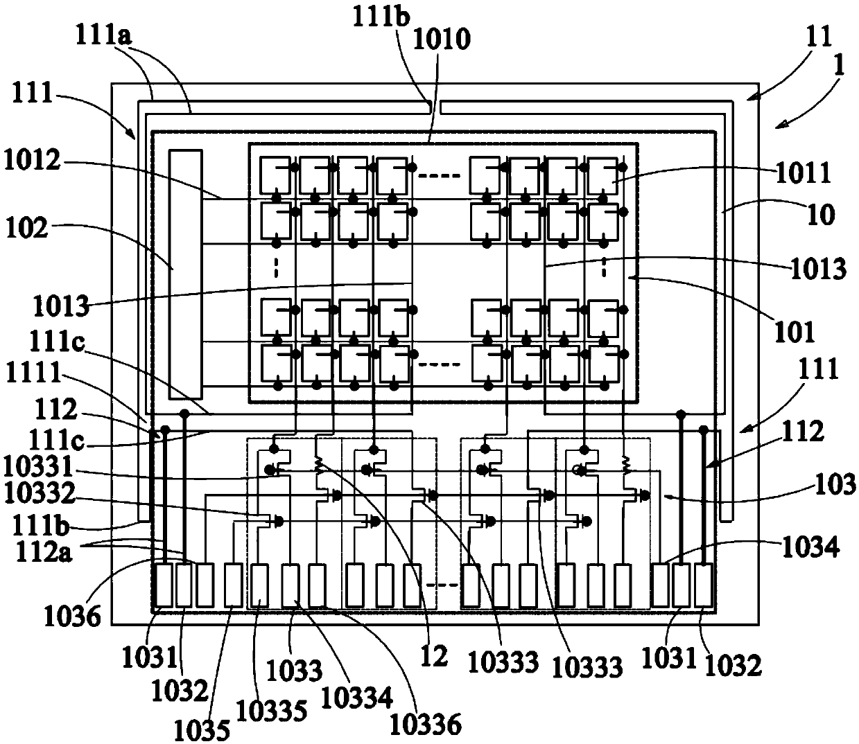
[0028] see figure 1 , which is a schematic diagram of the array substrate of the first embodiment of the present invention; as shown in the figure, this embodiment provides an array substrate 1, and the array substrate 1 includes an effective circuit area 10 and a layer crack detection wiring area 11. The effective circuit area 10 includes a pixel array circuit 102 and an array detection circuit 103. The pixel array circuit 101 includes a plurality of ...


PUM


Abstract

The invention discloses an array substrate, a display panel and a film layer crack detection method. The array substrate comprises an effective circuit area and a film layer crack detection wiring area. The effective circuit area comprises a pixel array circuit and an array detection circuit, and the pixel array comprises a plurality of sub-pixel circuits and a plurality of data lines, wherein thesub-pixel circuits and the data lines are arranged in an array, and each data line is connected with the plurality of sub-pixel circuits located in the same column / row. The array detection circuit comprises a plurality of sub-detection circuits, and each sub-detection circuit comprises a thin film transistor, and each sub-detection circuit is correspondingly connected with one data line through the corresponding thin film transistor. The film layer crack detection wiring area comprises a crack detection wire, wherein one end of the crack detection wire is connected with a data line of the sub-pixel circuit, and the other end of the crack detection wiring is connected with a sub-detection circuit corresponding to the data line. The crack detection wiring is arranged along the periphery ofthe effective circuit area. According to the invention, the array substrate with poor real-time interception can be realized.

Description

technical field [0001] The present invention relates to the technical field of array substrate manufacturing, and in particular to an array substrate, a display panel and a film layer crack detection method. Background technique [0002] Under the current glass cutting process in the production process, cutting cracks will occur around the cut array substrate. In the initial stage, there is no obvious abnormality in the array substrate with cracks around it, but with the subsequent environmental changes, such as after being subjected to various temperature, vibration, and pressure impacts, the cracks will aggravate, and the array substrate will be seriously damaged. The cracks and breakages of the array substrate will affect the circuit film layer of the array substrate and cause cracks, which will cause the signal line of the array substrate to be broken or micro-broken, which will lead to abnormal display or quality degradation of the array substrate. [0003] At present,...

Claims


Application Information

Patent Timeline
Patent Type & Authority Applications(China)
IPC IPC(8): H01L27/12H01L21/66H01L23/544
CPCH01L22/12H01L22/14H01L22/32H01L22/34H01L27/124
Inventor 张金方王欢刘权赵磊张露韩珍珍胡思明
Owner KUNSHAN GO VISIONOX OPTO ELECTRONICS CO LTD
Why Eureka
Try Eureka