Supercharge Your Innovation With Domain-Expert AI Agents!

Devices for high-speed imaging sensor data transfer

An imaging sensor and data signal technology, applied in the direction of instruments, scientific instruments, image communication, etc., can solve the problems of difficult and expensive manufacturing of a single main PCB

Active Publication Date: 2020-08-21
KLA CORP
View PDF8 Cites 0 Cited by
  • Summary
  • Abstract
  • Description
  • Claims
  • Application Information

AI Technical Summary

Problems solved by technology

Also, the total component count to make a single master PCB is usually lower than for a small modular board array
However, a single master PCB is subject to the additional design constraints of having high-speed data rates, making the fabrication of a single master PCB more difficult and more expensive than a small modular board array

Method used


Image

  • Devices for high-speed imaging sensor data transfer
  • Devices for high-speed imaging sensor data transfer
  • Devices for high-speed imaging sensor data transfer

Examples


Embodiment Construction

[0022] Reference will now be made in detail to the disclosed objects illustrated in the accompanying drawings.

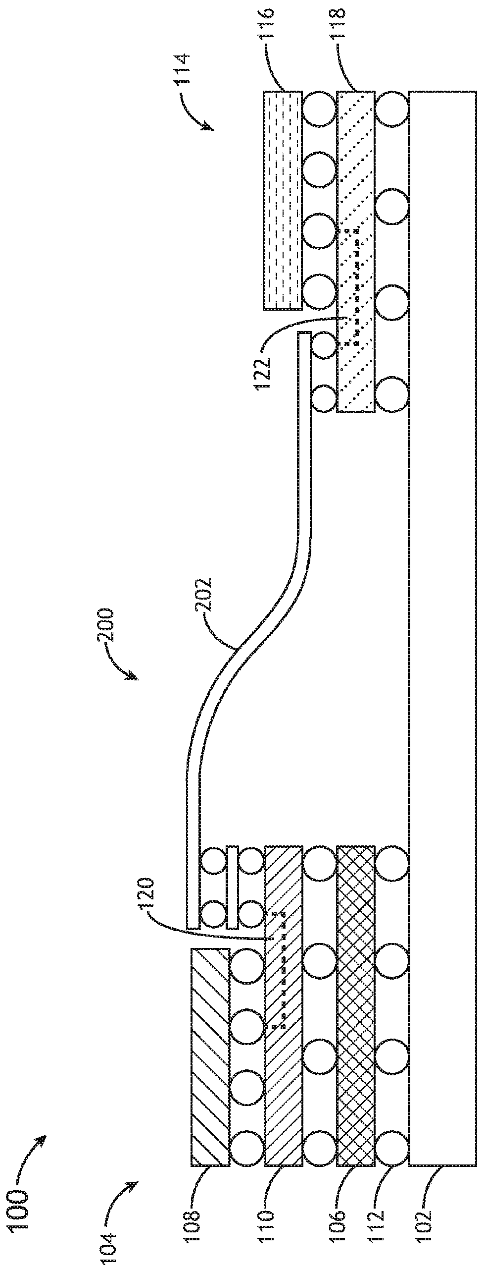
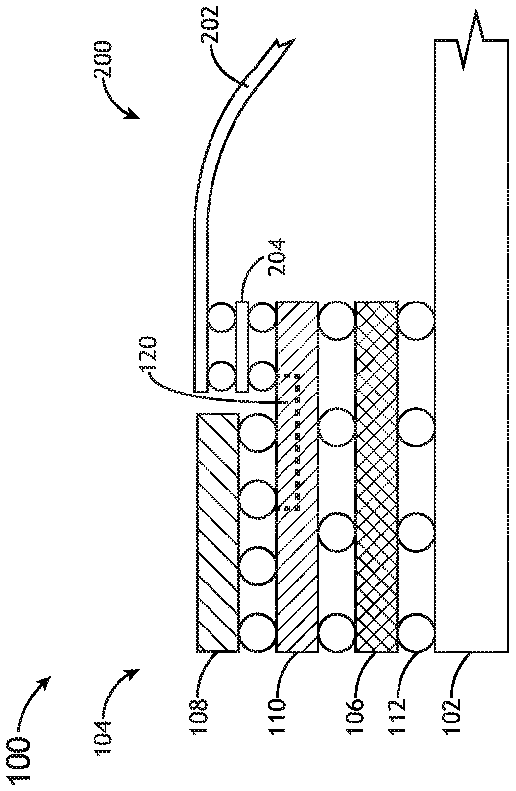
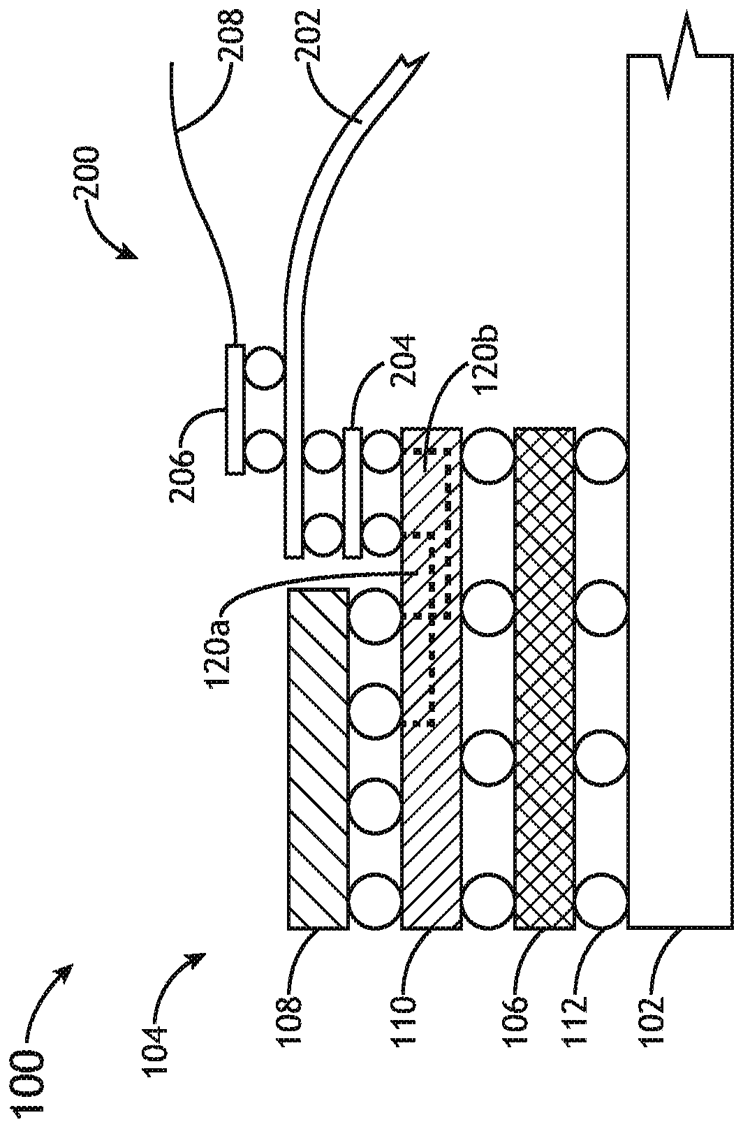
[0023] Usually refer to Figures 1 to 6 , according to one or more embodiments of the present invention, an assembly for high-speed image sensor data transfer is disclosed.

[0024] Embodiments of the invention relate to an image sensor assembly for high speed data transfer. Additional embodiments of the invention also relate to an imaging sensor and signal routing assembly for an image sensor assembly. Additional embodiments of the present invention relate to a high speed imaging system including an image sensor assembly for high speed data transfer. It should be noted herein that the terms "imaging sensor" and "scanning sensor" are considered equivalent for the purposes of the present invention. Additionally, it should be noted herein that for the purposes of the present invention, "inspection system" and "metric system" are considered equivalent systems.

[002...


PUM


Abstract

The present invention discloses an imaging sensor assembly comprising at least one substrate comprising a plurality of substrate signal lines. The imaging sensor assembly also includes at least one imaging sensor package disposed on the at least one substrate, the at least one imaging sensor package including at least one imaging sensor disposed on the at least one imaging sensor package substrate. The imaging sensor assembly also includes at least one receiver package disposed on the at least one substrate, the receiver package including at least one receiver integrated circuit disposed on the at least one receiver package substrate. The imaging sensor assembly also includes at least one electrical interconnect operably coupled to the at least one imaging sensor package and the at least one receiver package. A plurality of data signals are transmitted between the at least one imaging sensor package and the at least one receiver package via the at least one electrical interconnect.

Description

[0001] Cross References to Related Applications [0002] This application asserts under 35 U.S.C. §119(e) filed August 29, 2016 by Steve Zamek, David L. Brown, and Venkate U.S. Provisional Patent Application No. 62 / 380,742, entitled "METHOD FOR DATATRANSFER FROM A HIGH-SPEED SCANNING SENSOR," in which Venkatraman Iyer is the inventor Rights, said application is incorporated herein by reference in its entirety. technical field [0003] The present invention relates generally to imaging sensors suitable for implementation in semiconductor inspection and metrology systems, and more particularly, to high speed imaging sensor data transfer in semiconductor inspection and metrology systems. Background technique [0004] The demand for improved semiconductor device inspection and metrology systems continues to increase. For example, inspection systems typically include one or more imaging or scanning sensors that are part of an integrated circuit package. The integrated circuit...

Claims


Application Information

Patent Timeline
Patent Type & Authority Patents(China)
IPC IPC(8): H01L27/146H01L25/18H01L25/16H01L21/67H01L21/66
CPCH01J2237/2447G01N21/9501H01J2237/2441H01L27/14618H01L27/14636H04N23/56H01L21/67242H01L22/30H01L25/0657H01L25/16H01L25/18H01L27/14683H04N25/711H04N25/71G01T1/24H01J37/28
Inventor 史蒂夫(沙龙)·察梅克戴维·L·布朗芬卡特拉曼·伊艾
Owner KLA CORP
Features
  • R&D
  • Intellectual Property
  • Life Sciences
  • Materials
  • Tech Scout
  • Unparalleled Data Quality
  • Higher Quality Content
  • 60% Fewer Hallucinations
Learn More