
Method for grinding sample cross section

A grinding method and sample technology, applied in the preparation of test samples, grinding devices, grinding machine tools, etc., can solve the problems of small samples being difficult, unable to correct micro-samples, and difficult to obtain expected results, and achieve increased area and thickness. , the effect of simplifying the difficulty

Inactive Publication Date: 2019-04-26
SHANGHAI HUAHONG GRACE SEMICON MFG CORP
View PDF4 Cites 0 Cited by
  • Summary
  • Abstract
  • Description
  • Claims
  • Application Information

AI Technical Summary

Problems solved by technology

[0003] At present, due to the higher integration of analysis samples in the field of semiconductor failure analysis, the smaller the size, it is very difficult to fix, stick, and grind small samples in the process of grinding, and it is impossible to correct the level of micro samples, so it is difficult to get expectations. Effect

Method used


Image

  • Method for grinding sample cross section
  • Method for grinding sample cross section
  • Method for grinding sample cross section

Examples


Embodiment Construction

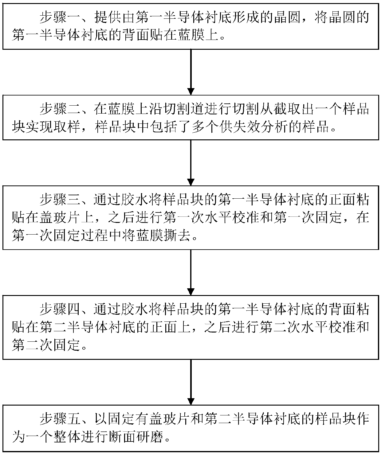
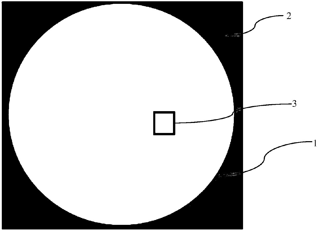
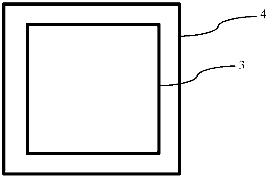
[0031] Such as figure 1 Shown is the flow chart of the cross-section grinding method of the sample of the embodiment of the present invention; Figure 2A to Figure 2D Shown is the schematic diagram of the structure in each step of the method of the embodiment of the present invention, the cross-section grinding method of the sample of the embodiment of the present invention comprises the following steps:

[0032] Step 1, such as Figure 2A As shown, a wafer formed by a first semiconductor substrate 1 is provided, on which a chip is formed, and a plurality of samples needing cross-section grinding are provided on the wafer, and each of the samples is used for failure analysis ; Paste the back side of the first semiconductor substrate 1 of the wafer on the blue film 2 ;

[0033] In the method of the embodiment of the present invention, the first semiconductor substrate 1 is a silicon substrate,

[0034] Step two, such as Figure 2A As shown, sampling is carried out, and the ...


PUM

PropertyMeasurementUnit
Thicknessaaaaaaaaaa

Abstract

The invention discloses a method for grinding a sample cross section. The method for grinding the sample cross section comprises the steps that firstly, wafer formed by first semiconductor substrate is provided, and the reverse side of the first semiconductor substrate of wafer is attached to blue film; secondly, sampling is conducted, wherein cutting is conducted in a cutting way on the upper edge of the blue film, thus a sample block is acquired, and the sample block comprises multiple samples for failure analysis; thirdly, the front side of the first semiconductor substrate of the sample block is stuck on cover glass through glue, then first horizontal calibrating and first fixing are conducted, and the blue film is torn off in first fixing process; fourthly, the reverse side of the first semiconductor substrate of the sample block is stuck on the front side of second semiconductor substrate through glue, then second horizontal calibrating and second fixing are conducted; and fifthly, cross section grinding is conducted with the sample block fixed with the cover glass and the second semiconductor substrate as a whole. By means of the method for grinding the sample cross section,grinding difficulty of the sample cross section can be simplified, and grinding of cross sections of minitype samples is achieved.

Description

technical field [0001] The invention relates to a semiconductor integrated circuit manufacturing method, in particular to a sample cross-section grinding method. Background technique [0002] In the field of semiconductor failure analysis, due to the small structure or different materials to be analyzed in the process of silicon wafer production, testing, and product analysis, manual splitting and fixed-point cutting cannot meet the analysis requirements, and samples can only be obtained by cross-section grinding. specific analysis results. [0003] At present, due to the higher integration of analysis samples in the field of semiconductor failure analysis, the smaller the size, it is very difficult to fix, stick, and grind small samples in the process of grinding, and it is impossible to correct the level of micro samples, so it is difficult to get expectations. Effect. Contents of the invention [0004] The technical problem to be solved by the present invention is to ...

Claims


Application Information

Patent Timeline
IPC IPC(8): B24B1/00B24B37/00B24B37/27G01N1/28
Inventor 裘莺陆文菊
Owner SHANGHAI HUAHONG GRACE SEMICON MFG CORP
Learn More