Interconnect substrate having cavity for stackable semiconducotr assembly as well as manufacturing method thereof

A technology for interconnecting substrates and semiconductors, used in semiconductor/solid-state device manufacturing, semiconductor devices, semiconductor/solid-state device components, etc. Effect of Interconnection Distance

Inactive Publication Date: 2019-04-26
BRIDGE SEMICON
View PDF2 Cites 0 Cited by
  • Summary
  • Abstract
  • Description
  • Claims
  • Application Information

AI Technical Summary

Problems solved by technology

However, since solder balls are usually spherical after reflow, large solder balls that meet the required height will result in larger board size
Therefore, using solder balls as vertical connections does not meet the stringent requirements of mobile devices

Method used


Image

  • Interconnect substrate having cavity for stackable semiconducotr assembly as well as manufacturing method thereof
  • Interconnect substrate having cavity for stackable semiconducotr assembly as well as manufacturing method thereof
  • Interconnect substrate having cavity for stackable semiconducotr assembly as well as manufacturing method thereof

Examples


Embodiment 1

[0103] Figure 1-14 It is a diagram of a manufacturing method of an interconnect substrate in the first embodiment of the present invention. The interconnect substrate includes a core layer, a build-up circuit, a reinforcement layer, a series of metal pillars and a cavity.

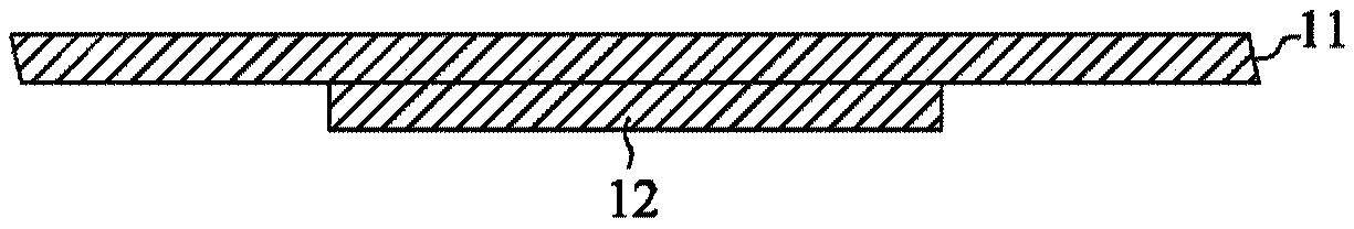
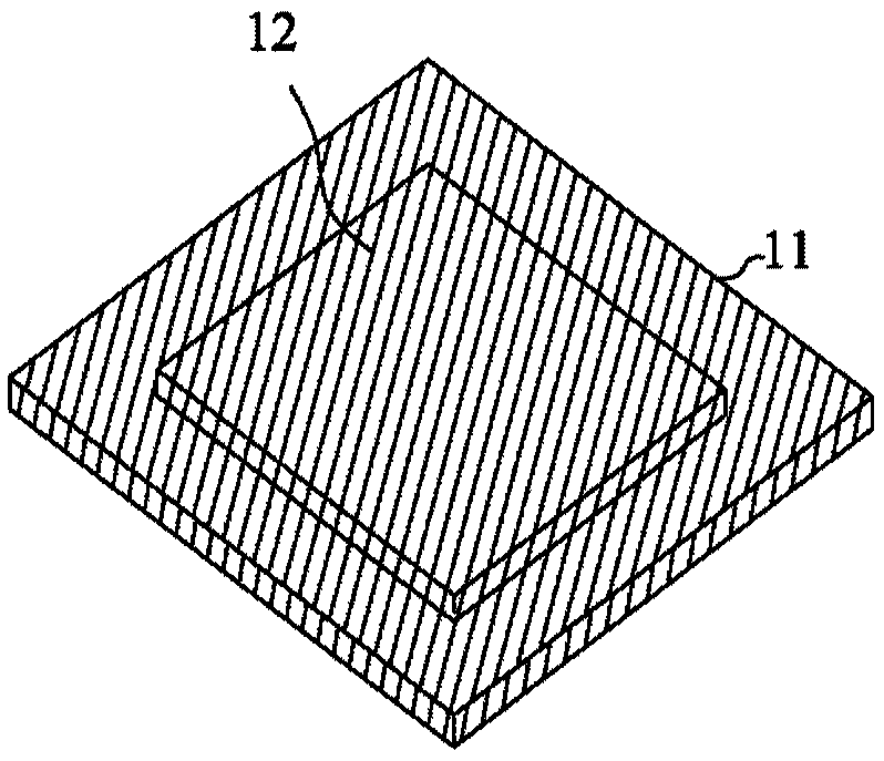
[0104] figure 1 and 2 They are respectively a cross-sectional view and a perspective view of the bottom of the metal bump layer 12 formed on the metal carrier 11 . The metal carrier 11 and the metal bump layer 12 are generally made of copper, aluminum, nickel, stainless steel, or other metals or alloys. The material of the metal bump layer 12 can be the same as or different from the metal carrier 11 . The metal carrier 11 may have a thickness of 0.05 mm to 0.5 mm (preferably 0.1 mm to 0.2 mm), and the metal bump layer 12 may have a thickness of 10 microns to 100 microns. In this embodiment, the metal carrier 11 is made of copper and has a thickness of 0.15 mm, and the metal bump layer 12 is made of cop...

Embodiment 2

[0120] Figure 20-26 It is a diagram of the manufacturing method of the interconnection substrate according to the second embodiment of the present invention, and the core layer is further provided with auxiliary metal pads.

[0121] For the purpose of brief description, any descriptions in the above-mentioned embodiment 1 that can be used for the same application are incorporated here, and it is not necessary to repeat the same descriptions.

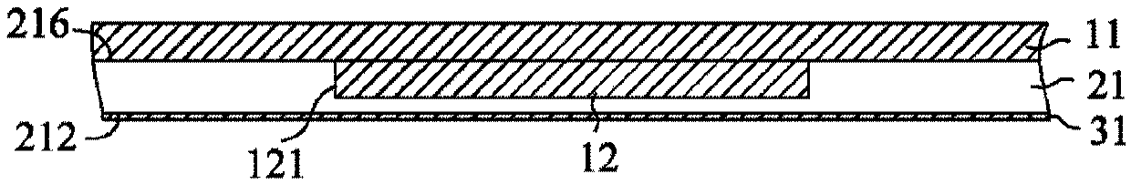
[0122] Figure 20 It is a cross-sectional view of the metal bump layer 12 and the arrayed auxiliary metal pads 13 formed on the metal carrier 11 . The metal bump layer 12 and the auxiliary metal pad 13 extend downward from a surface of the metal carrier 11 and have the same thickness. The material of the auxiliary metal pad 13 can be the same as the material of the metal bump layer 12, and can be formed by a patterned deposition method, such as electroplating, electroless plating, evaporation, sputtering or a combination thereof, or b...

Embodiment 3

[0135] Figure 31-37 It is a diagram of the manufacturing method of the interconnect substrate according to the third embodiment of the present invention, which is provided with routing lines exposed from the cavity.

[0136] For the purpose of brief description, any descriptions in the above embodiments that can be used for the same application are incorporated here, and the same descriptions do not need to be repeated.

[0137] Figure 31 for Figure 20 A cross-sectional view of routing lines 311 formed on the metal bump layer 12 in FIG. The routing lines 311 are usually made of copper and can be formed by patterned deposition by various techniques, such as electroplating, electroless plating, evaporation, sputtering or a combination thereof, or by thin film deposition followed by a metal patterning step And formed.

[0138] Figure 32 It is a cross-sectional view of the core layer 21 formed on the metal carrier 11 , the metal bump layer 12 , the auxiliary metal pad 13 ...


PUM


Abstract

An interconnect substrate includes vertical connection channels around a cavity. The vertical connection channels are made of a combination of metal posts and metallized vias. The cavity includes a recess in a core layer and an aperture in a stiffener. The metal posts, disposed over the top surface of the core layer, are sealed in the stiffener and are electrically connected to a buildup circuitryadjacent to the bottom surface of the core layer. The minimal height of the metal posts needed for the vertical connection can be reduced by the amount equal to the depth of the recess. The buildup circuitry is electrically connected to the metal posts through the metallized vias.

Description

technical field [0001] The present invention relates to an interconnection substrate and a method for making the same, in particular to an interconnection substrate with cavities surrounded by a series of vertical connection channels, and these vertical connection channels are made of Combination of metal pillars and metallized blind holes. Background technique [0002] The market trend of multimedia devices tends to be faster and thinner. One of the methods is to stack multiple components on the circuit board to improve electrical performance and achieve minimum form-factor. For example, US Pat. No. 7,894,203 discloses a circuit board with a cavity for this purpose, and electroplated metal posts are arranged around the cavity. However, since it is difficult to form metal pillars with a high aspect ratio opening (that is, tall and thin metal pillars) by electroplating, voids at the metal pillars or insufficient bonding strength may lead to unconnected I / Os, components Pro...

Claims


Application Information

Patent Timeline
Patent Type & Authority Applications(China)
IPC IPC(8): H01L23/492H01L23/498H01L21/48
CPCH01L2224/16225H01L23/492H01L21/4821H01L23/49822H01L23/49833
Inventor 林文强王家忠
Owner BRIDGE SEMICON
Why Eureka
Try Eureka