
Channel integrated engineering implementation method and device

An implementation method and engineering technology, which is applied in the direction of impedance network, digital technology network, electrical components, etc., can solve the problems of complex architecture and large consumption of FPGA hardware resources, and achieve the effect of reducing usage and strong engineering realizability

Active Publication Date: 2019-04-26
CHINA ELECTRONIC TECH GRP CORP NO 38 RES INST
View PDF4 Cites 0 Cited by
  • Summary
  • Abstract
  • Description
  • Claims
  • Application Information

AI Technical Summary

Problems solved by technology

[0004] The technical problem to be solved by the present invention is: the structure of the current integrated channel engineering is complex and the consumption of FPGA hardware resources is large, and a method and device for implementing integrated channel engineering are provided

Method used


Image

  • Channel integrated engineering implementation method and device
  • Channel integrated engineering implementation method and device
  • Channel integrated engineering implementation method and device

Examples


Embodiment Construction

[0026] The embodiments of the present invention are described in detail below. This embodiment is implemented on the premise of the technical solution of the present invention, and detailed implementation methods and specific operating procedures are provided, but the protection scope of the present invention is not limited to the following implementation example.

[0027] In this embodiment, from the perspective of complex bandpass filters, the functional block diagram of data channel synthesis is as follows figure 1 shown. According to this principle, the polyphase structure of channel synthesis can be deduced as:

[0028]

[0029] Where j=0,1,...,M-1, K=2M, M is the extraction rate, and K is the number of channels. Analyzing the above formula, it can be found that

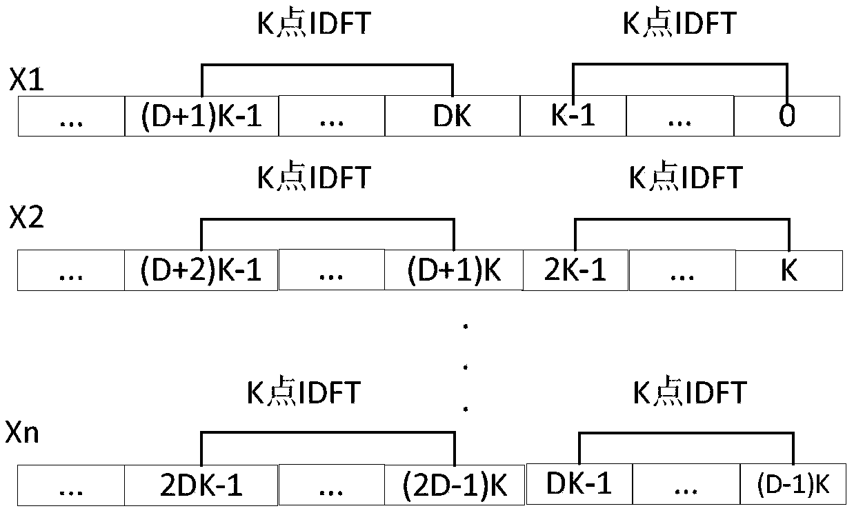
[0030] (1) yes K point IDFT;

[0031] (2) Since K=2M,

[0032] (3) is the polyphase filtering result of the IDFT output and the prototype filter.

[0033] Based on the above analysis, a channel ...


PUM


Abstract

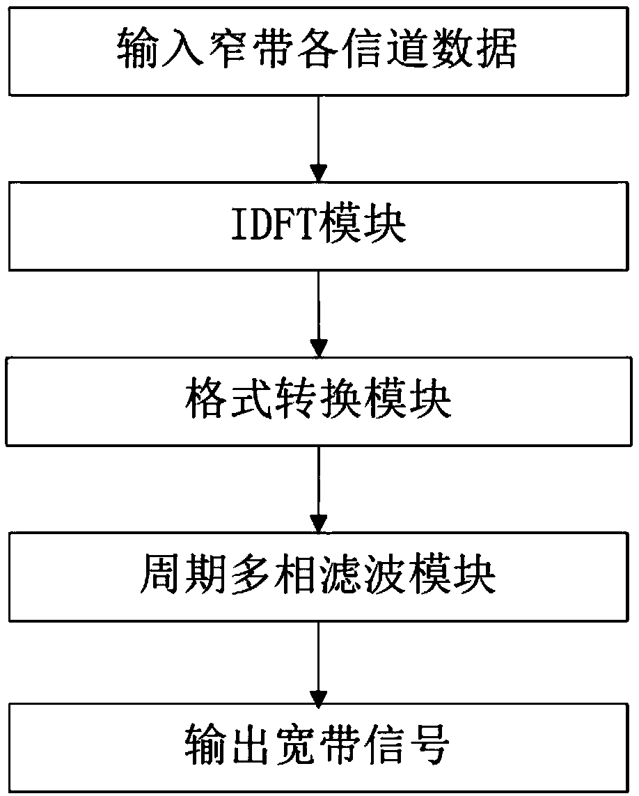
The invention discloses a channel integrated engineering implementation method and device. The method comprises the following steps: firstly performing a joint IDFT on a plurality of input narrowbandchannel data, and obtaining the results of positive and negative paths through data selection; then performing format conversion on the output data of each path such that the subsequent filter can multiplex the multiplier and the data is output in a natural order after filtering; finally, periodically switching the positive and negative data for multiphase filtering, and outputting a wideband signal. The device comprises an inverse discrete Fourier transform (IDFT) module, a format conversion module, and a periodic poly-phase filtering module. The invention realizes the IDFT of the odd-numbered channel multiplication-1 data by using direct IDFT, and adopts the cyclic switching data source for the multi-phase filtering, which greatly reduces the use of multiplier resources, with strong engineering achievability. The invention solves the problem that the signal phase is abrupt caused by direct IDFT for channel synthesis, and the integrated wideband signal waveform error is within the engineering acceptable range, which satisfies the subsequent broadband signal processing requirements.

Description

technical field [0001] The invention relates to the field of broadband signal synthesis, in particular to a channel synthesis engineering realization method that requires broadband signal synthesis after the broadband signal is channelized. Background technique [0002] With the rapid development of electronic information technology and radio technology, many systems have an increasing demand for spectrum bandwidth. However, there are many difficulties in the processing of broadband signals, and channelization has become one of the choices for broadband signal processing design. After channelizing the wideband signal, many systems need to restore the narrowband signal to a wideband signal for further signal processing. The process of synthesizing multiple narrowband signals into wideband signals is channel synthesis. [0003] Channel synthesis has broad application prospects in electronic reconnaissance receivers and communication receivers, and can be used for non-uniform...

Claims


Application Information

Patent Timeline
Patent Type & Authority Applications(China)
IPC IPC(8): H04B1/16H03H17/02
CPCH03H17/0201H04B1/16
Inventor 靳学明王小静吕新正蒋千张锦中万卫华
Owner CHINA ELECTRONIC TECH GRP CORP NO 38 RES INST
Learn More