An erasing method of a single-grid non-volatile memory

A non-volatile memory technology, applied in information storage, static memory, read-only memory, etc., can solve the problems of serious over-erasing, increased cost, and complicated manufacturing process

Inactive Publication Date: 2019-04-30
YIELD MICROELECTRONICS CORP
View PDF6 Cites 0 Cited by
  • Summary
  • Abstract
  • Description
  • Claims
  • Application Information

AI Technical Summary

Problems solved by technology

Therefore, in the structure of the known non-volatile memory, in addition to the gate layer of the transistor, an additional conductive layer needs to be added to store charges, and a double-layer structure is formed. There are more steps in the process of film deposition, etching, exposure and development, etc., which increase the cost, complicate the process, reduce the yield of components, and increase the man-hours, especially when used in embedded (Embedded) EEPROM products.
[0004] In the known erasing method for EEPROM components, the stored charge is moved from the floating gate to the transistor under the tunneling effect of the Fowler-Nordheim (Fowler-Nordheim) tunneling (referred to as F-N tunneling) technology. In addition, the voltage often needs to be greater than 10V, and because the structure of the single-gate EEMPROM memory is transistor substrate-floating gate-capacitor substrate, the stored charge can be released to any direction according to the direction of the electric field; resulting in a single-gate Over-erasing of EEPROM components becomes more serious

Method used


Image

  • An erasing method of a single-grid non-volatile memory
  • An erasing method of a single-grid non-volatile memory
  • An erasing method of a single-grid non-volatile memory

Examples


Embodiment Construction

[0043] The following will clearly and completely describe the technical solutions in the embodiments of the present invention with reference to the accompanying drawings in the embodiments of the present invention. Obviously, the described embodiments are only some, not all, embodiments of the present invention. Based on the embodiments of the present invention, all other embodiments obtained by persons of ordinary skill in the art without making creative efforts belong to the protection scope of the present invention.

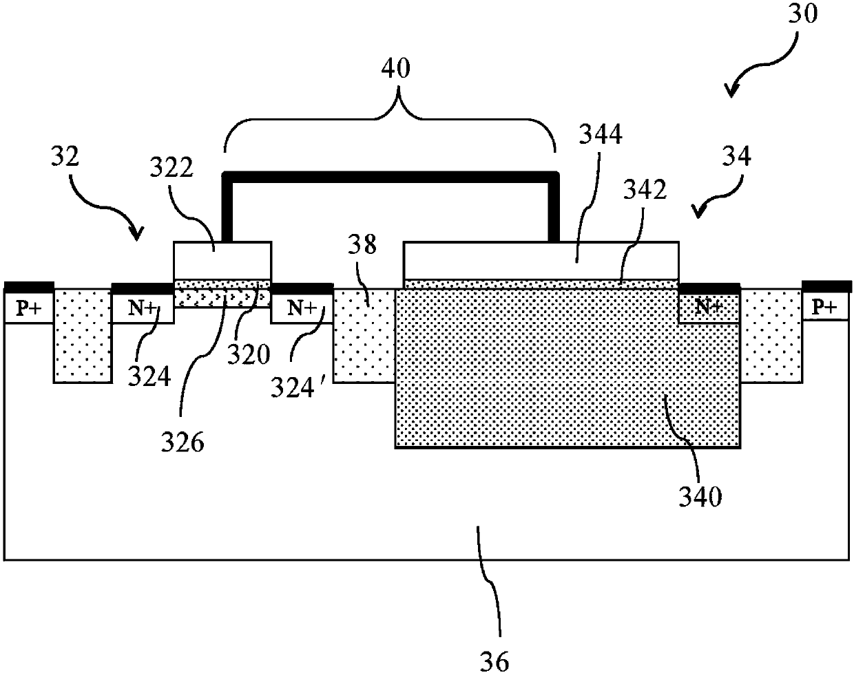
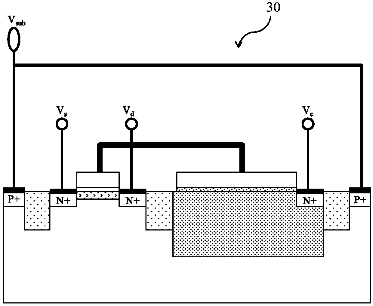
[0044] Figure 1A A cross-sectional view of the single-gate non-volatile memory structure provided by the first embodiment of the present invention, the single-gate non-volatile memory structure 30 includes an NMOS transistor (NMOSFET) 32 and an N-well (N-well) capacitor 34, In the P-type silicon substrate 36; the NMOS transistor 32 includes a first dielectric layer 320 located on the surface of the P-type silicon substrate 36, a first conductive gate 322 stack...


PUM


Abstract

The invention discloses an erasing method of a single-grid non-volatile memory. The non-volatile memory is provided with a single floating gate structure, when erasing operation is carried out, voltage is applied to a drain electrode, voltage is not applied to a gate electrode, a reverse layer is generated and controlled through the drain electrode voltage, and therefore the erasing voltage is reduced, the erasing speed is increased, and the problem of excessive erasing can be prevented.

Description

technical field [0001] The present invention relates to a kind of non-volatile memory (Non-Volatile Memory), in particular to a kind of oxide layer (oxide) thickness greater than 100 Angstroms that can be used in high pressure process An erasing method for single-gate non-volatile memory for erasing storage elements. Background technique [0002] Currently, Complementary Metal Oxide Semiconductor (CMOS) process technology has become a common manufacturing method for application specific integrated circuits (ASICs). Today, with the development of computer information products, Electronically Erasable Programmable Read Only Memory (Electrically Erasable Programmable Read Only Memory, EEPROM) has the function of electrically writing and erasing data due to its non-volatile memory function, and when the power is turned off The final data will not disappear, so it is widely used in electronic products. [0003] Non-volatile memory is programmable to store charge to change the ...

Claims


Application Information

Patent Timeline
Patent Type & Authority Applications(China)
IPC IPC(8): G11C16/14
CPCG11C16/14
Inventor 林信章黄文谦骆玮彤
Owner YIELD MICROELECTRONICS CORP
Why Eureka
Try Eureka