Operation method of silion nitride read-only memory element

A technology of read-only storage element and operation method, which is applied in the direction of electrical components, semiconductor/solid-state device manufacturing, circuits, etc., can solve leakage (leakage, large current, etc.) problems, increase substrate effect, increase performance, and prevent excessive erasure Effect

Inactive Publication Date: 2008-06-25
MACRONIX INT CO LTD
View PDF3 Cites 0 Cited by
  • Summary
  • Abstract
  • Description
  • Claims
  • Application Information

AI Technical Summary

Problems solved by technology

[0004] However, as semiconductor devices continue to be miniaturized, the gate line width will gradually shrink, which will cause problems in the operation of silicon nitride read-only memory devices, such as requiring a large current for programming operations; and especially When erasing (erasing), because holes (holes) are locally injected in the channel close to the source or drain, especially after multiple erasing, because of the accumulation above the source or drain There are a lot of holes, so there will be serious leakage (leakage) for the electrons of another bit that uses the same bit line or word line, especially at high temperatures. This is the so-called "over-erasing (over- erase)”
Moreover, the above situation will also be more serious after the initial voltage is reduced or the channel length is shortened.

Method used


Image

  • Operation method of silion nitride read-only memory element
  • Operation method of silion nitride read-only memory element

Examples


Embodiment Construction

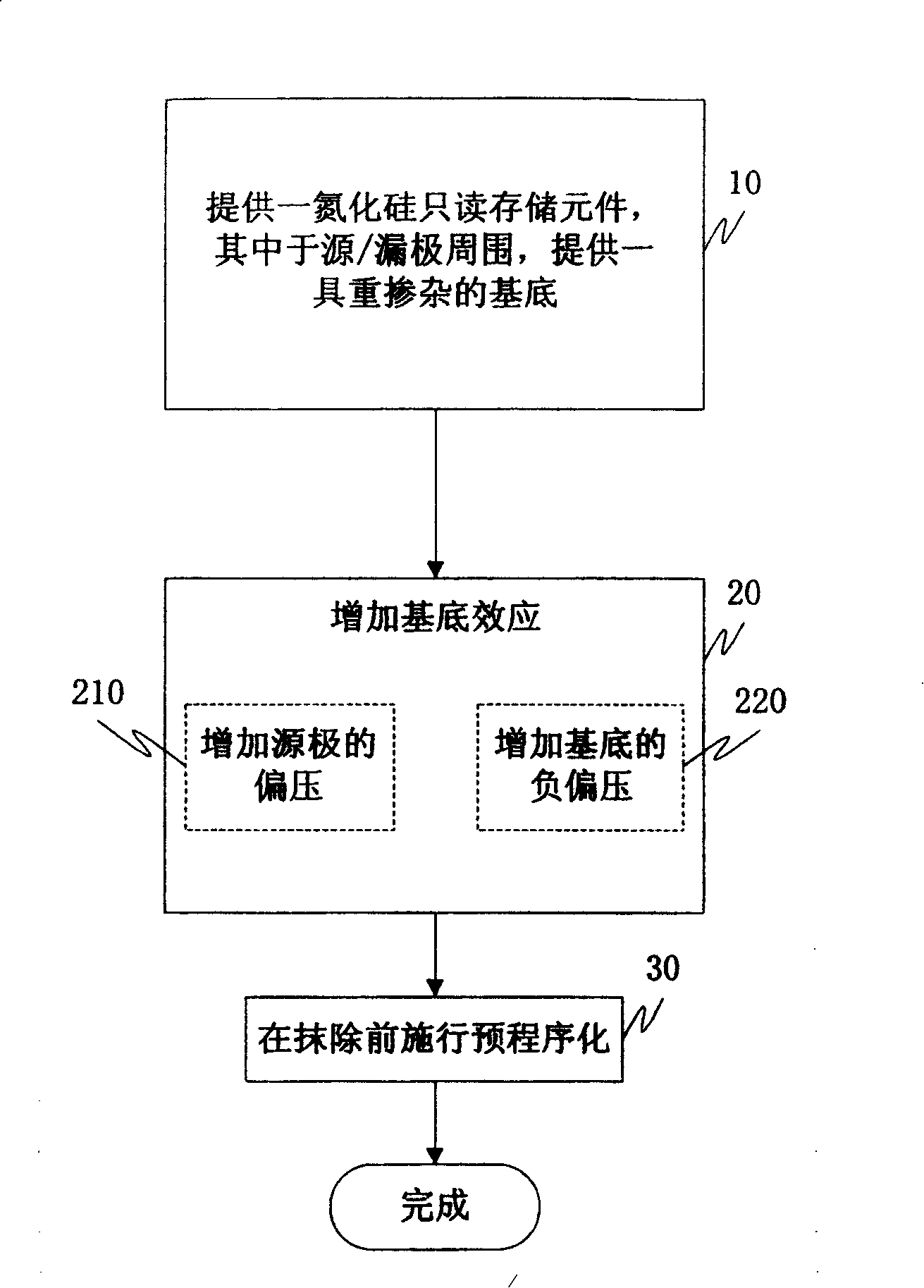
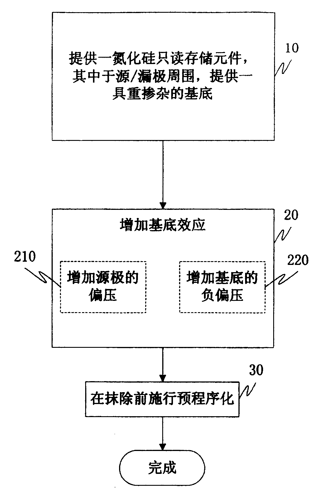
[0016] This embodiment mainly takes a silicon nitride read only memory device (NROM device for short) as an example, and as the device continues to shrink, the mechanism for executing the programming of the silicon nitride read only memory device is based on channel heat Electron injection (channel hotel electron injection, referred to as CHEI) method is the main method, and its operation steps are as follows figure 1 shown.

[0017] figure 1 It is an operation flow chart of a silicon nitride read-only memory device (NROM device) according to a preferred embodiment of the present invention.

[0018] Please refer to figure 1 , in step 10, a silicon nitride read-only memory device is provided, wherein a heavily doped substrate is provided around the source / drain. Since one of the purposes of the present invention is to reduce the programming current, the reduction of the programming current will affect the programming efficiency. Therefore, it is necessary to make the substr...


PUM


Abstract

The user of silicon nitride read-only memory elements is that a heavy doping base is provided for surroundings of source electrode / drain electrode. When programming, a relative plus source bias-voltage or a relatively minus base bias-voltage are used for increasing base effect and reducing the electric current of channel hot electron injection program. Before erasing of array of silicon nitride read-only memory element, a pre-programming is applied for all memory units to prevent over erasion.

Description

technical field [0001] The present invention relates to a method for operating a read-only memory device, and in particular to a method for operating a silicon nitride read-only memory device (NROM device for short). Background technique [0002] The current silicon nitride read-only memory element uses a stacked structure composed of a silicon oxide / silicon nitride / silicon oxide (ONO) composite layer as a charge trapping layer, while silicon oxide / silicon nitride / silicon oxide The (ONO) layer has a gate and a source / drain in the substrate adjacent to the gate. Because the material of the charge trapping layer is mainly silicon nitride, this kind of electrically erasable and programmable read-only memory (electrically erasable programmable ROM) is also called silicon nitride read-only memory (NROM). [0003] Since the silicon nitride layer has the effect of capturing charges, the electrons injected into the silicon nitride layer are not evenly distributed in the entire sili...

Claims


Application Information

Patent Timeline
Patent Type & Authority Patents(China)
IPC IPC(8): H01L21/8246
Inventor 刘承杰熊黛良陈家兴
Owner MACRONIX INT CO LTD
Why Eureka
Try Eureka