Semiconductor failure location test unit and failure location method thereof

A technology of failure location and test unit, which is applied in semiconductor/solid-state device testing/measurement, semiconductor devices, semiconductor/solid-state device components, etc., which can solve the problem of time-consuming and labor-intensive capture of failure locations, FA failure location, and unfavorable FIB interception of separated areas And other issues

Active Publication Date: 2019-04-30
SHANGHAI HUALI INTEGRATED CIRCUTE MFG CO LTD
View PDF2 Cites 4 Cited by
  • Summary
  • Abstract
  • Description
  • Claims
  • Application Information

AI Technical Summary

Problems solved by technology

[0003] The conventional snake-comb testkey structure puts all metals on the same layer, and the interlaced structure is not conducive to intercepting separated areas with FIB
After a short circu

Method used


Image

  • Semiconductor failure location test unit and failure location method thereof
  • Semiconductor failure location test unit and failure location method thereof
  • Semiconductor failure location test unit and failure location method thereof

Examples


Embodiment Construction

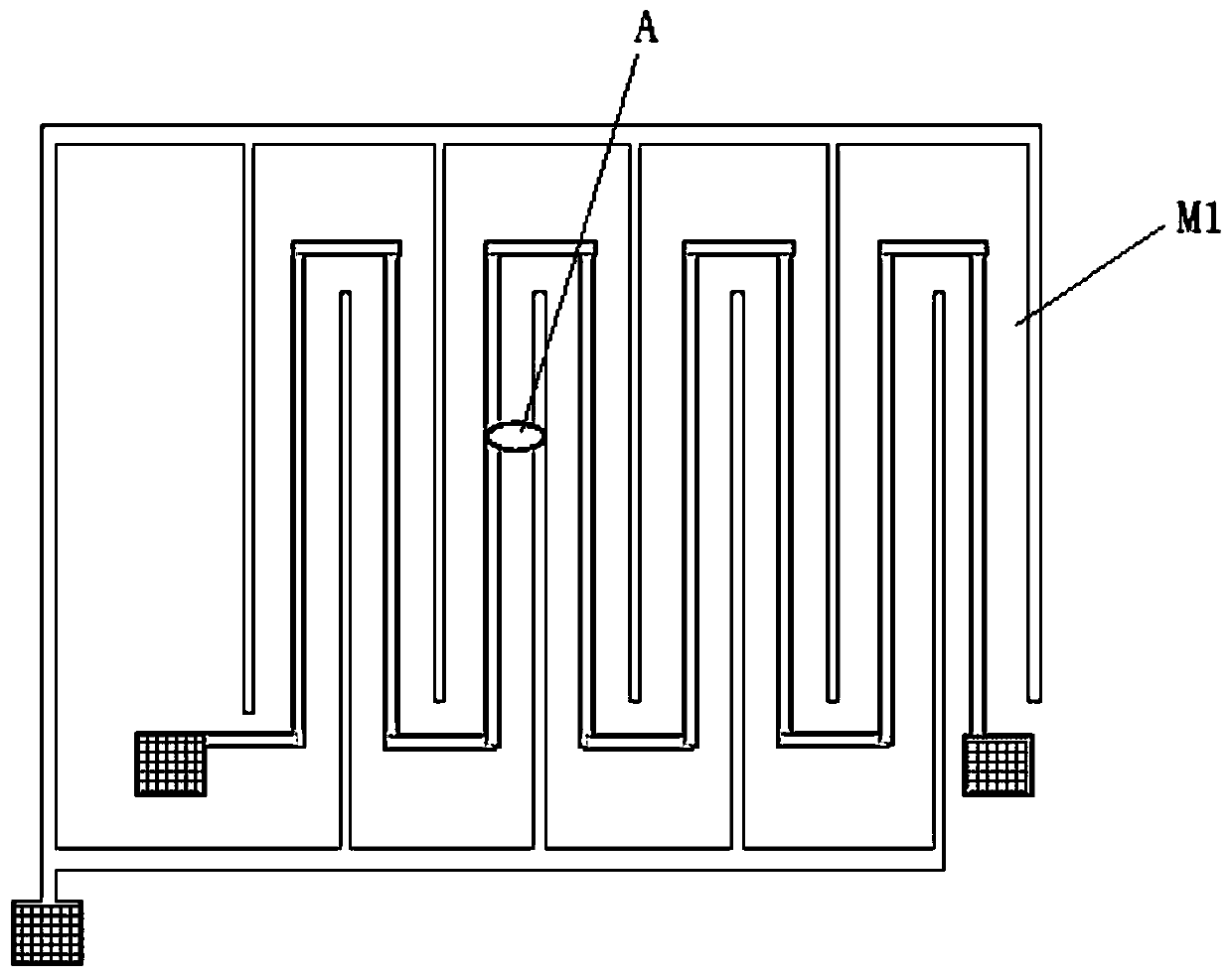
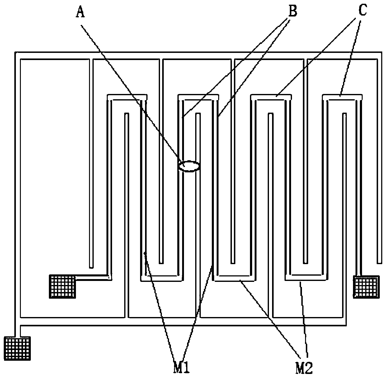
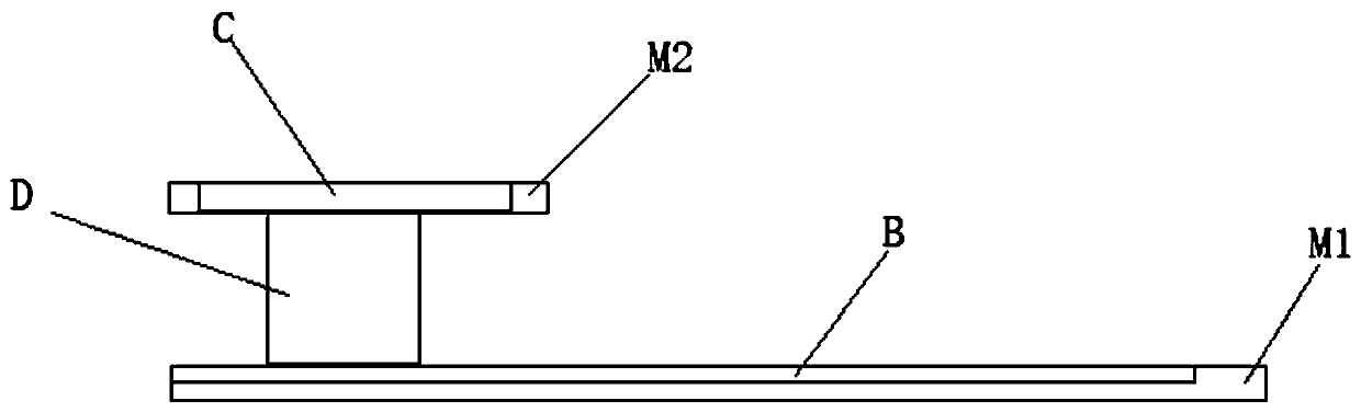
[0032] Such as figure 2 , image 3 As shown, the first embodiment of the semiconductor failure localization test unit (Snake-Comb testkey) provided by the present invention, the test unit is a comb structure located in the metal layer, and the bonding wire of the test unit is divided into the first Type bonding wire B and second type bonding wire C, adjacent first type bonding wires B are connected by second type bonding wire C, the length of the first type bonding wire B is longer than the second type class bonding wire C;

[0033] The applicant's division of the first type of bonding wire B and the second type of bonding wire C is based on figure 2 Take an example for further explanation. The arrangement direction of the first type of bonding wire B is the first direction, figure 2 Middle is the vertical direction. The arrangement direction of the second type of bonding wire C is the second direction, figure 2 Middle is the horizontal direction. The second type of...


PUM


Abstract

The invention discloses a semiconductor failure location test unit, which is a snake-comb structure in a metal layer. The bonding lines of the test unit are divided into first-type bonding lines and second-type bonding lines. The adjacent first-type bonding lines are connected through the second-type bonding lines. The first-type bonding lines are longer than the second-type bonding lines. The first-type bonding lines are arranged in a metal line I, the second-type bonding lines are arranged in a metal line II, and the metal layer I and the metal layer II are different metal layers. The invention also discloses a semiconductor failure location method. According to the semiconductor failure location test unit and the failure location method thereof of the invention, a semiconductor failurelocation test unit at a failure point (a hot spot) can be quickly and accurately grasped by using the existing failure location analysis instrument.

Description

technical field [0001] The invention relates to the field of semiconductors, in particular to a semiconductor failure location testing unit added to a fixed position of the wafer for process monitoring during wafer processing. The invention also relates to a method for semiconductor failure location by using the semiconductor failure location testing unit. Background technique [0002] With the reduction of the semiconductor process and the reduction of the operating voltage of low-power products, the short-circuit leakage current of the metal layer of the snake-comb testkey structure has also become very small. The 28nm process is at the microampere or even nanoampere level, which is not easy to be detected by conventional EMMI / OBIRCH / THERMAL and other testing instruments capture the hotspot; especially when this structure is placed on the metal 1 layer, since there are still various test structures under metal 1, such as SiGe and Poly local protrusions cause metal 1short,...

Claims


Application Information

Patent Timeline
IPC IPC(8): H01L21/66H01L23/522
CPCH01L22/12H01L23/522
Inventor 李金
Owner SHANGHAI HUALI INTEGRATED CIRCUTE MFG CO LTD
Why Eureka
Try Eureka