Wafer turnover device and wafer turnover method

A wafer and circumference technology, applied in the field of wafer turnover devices, can solve problems such as low efficiency, low manufacturing efficiency, wafer particle pollution, etc., and achieve the effects of convenient operation and production, improved qualification rate, and compact structure

Active Publication Date: 2019-05-03
上海福赛特机器人股份有限公司
View PDF4 Cites 3 Cited by
  • Summary
  • Abstract
  • Description
  • Claims
  • Application Information

AI Technical Summary

Problems solved by technology

If the wafer handling cannot be properly scheduled, it will easily lead to waste of time and low manufacturing efficiency.
[0003]In addition, the wafer is divided into front and back, and the front of the wafer must not be touched. The back of the wafer in the tray is placed on the carrier tray of the next process, which is labor-intensive and very inefficient
When placing the wafer, since the wafer has a flat edge in the circumferential direction, there are requirements for the placement direction of the flat edge when placing the wafer on different carriers, resulting in low efficiency when placing the wafer manually
Further, manual turnover of wafers still poses the risk of wafer particle contamination

Method used


Image

  • Wafer turnover device and wafer turnover method
  • Wafer turnover device and wafer turnover method
  • Wafer turnover device and wafer turnover method

Examples


Embodiment Construction

[0029] In order to make the content of the present invention clearer and easier to understand, the content of the present invention will be further described below in conjunction with the accompanying drawings. Of course, the present invention is not limited to this specific embodiment, and general replacements known to those skilled in the art are also covered within the protection scope of the present invention.

[0030] In the following description, many specific details are set forth in order to fully understand the present invention, but the present invention can also be implemented in other ways than those described here, so the present invention is not limited by the specific embodiments disclosed below.

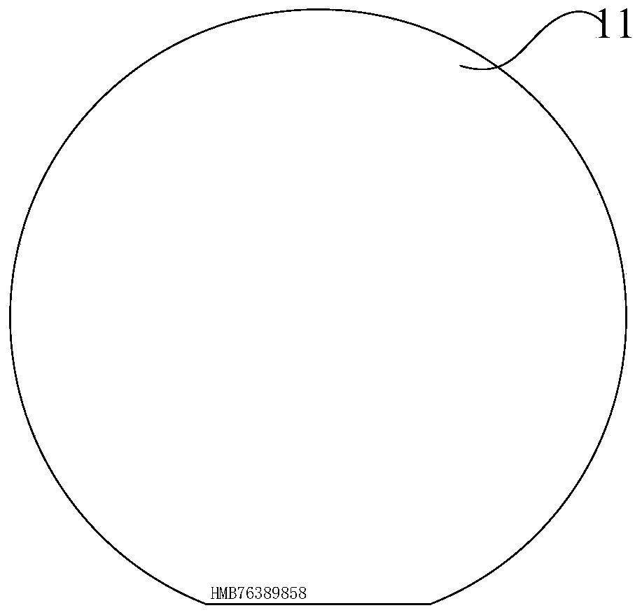
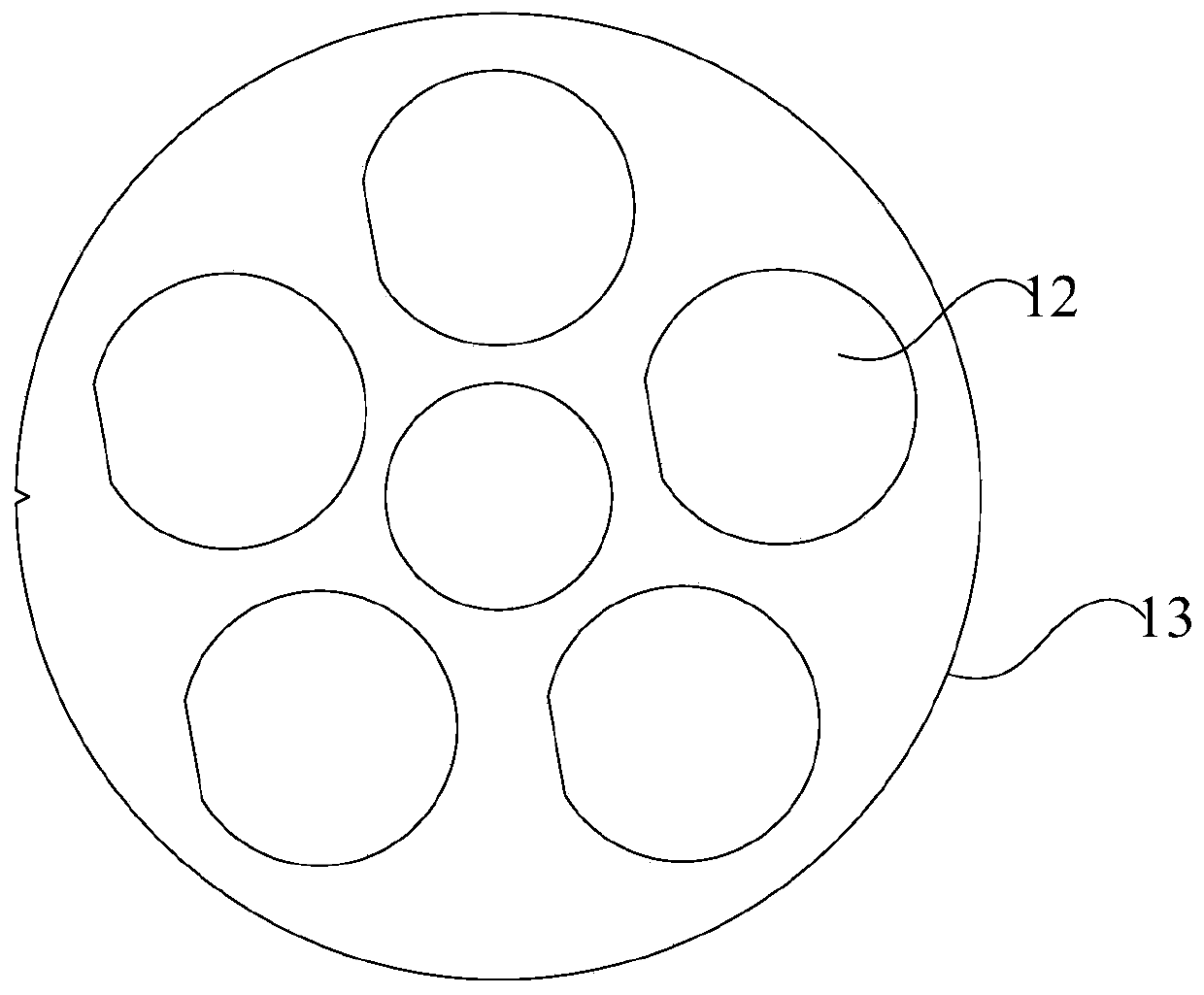
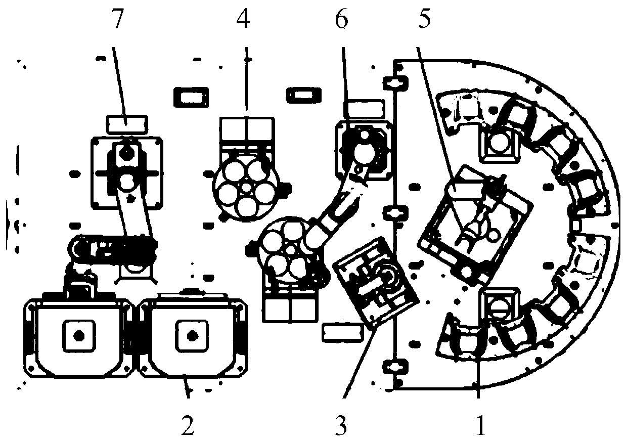
[0031] The following will combine Figure 1-Figure 5 The wafer turnaround device and the wafer turnaround method of the present invention will be described in detail. The wafer turnover device includes: a wafer cassette mounting table 1, a wafer disk mounting table 2...


PUM


Abstract

The invention discloses a wafer turnover device and a wafer turnover method. The wafer turnover device comprises a wafer box carrying table, a wafer disc carrying table, a first transfer table, a second transfer table, three carrying mechanisms and a control unit. The first transfer table comprises a wafer edge finder for identifying and adjusting the flat edge position of a wafer; and the secondtransfer table comprises a wafer disc edge finder for identifying and adjusting the flat edge position of a bearing part of a wafer disc. The control unit controls the three carrying mechanisms to transfer wafers between the wafer box carrying table and the wafer edge finder, between the wafer edge finder and the wafer disc edge finder and between the wafer disc edge finder and the wafer disc carrying table, so that the wafers can be efficiently carried from the wafer box carrying table to the wafer disc carrying table or from the wafer disc carrying table to the wafer box carrying table.

Description

technical field [0001] The invention relates to the technical field of semiconductor wafer manufacturing, in particular to a wafer turnover device and a wafer turnover method. Background technique [0002] In the production of the semiconductor industry, wafers use different production processes in the manufacturing process, and the wafer carriers used in the production equipment of different production processes are different. Therefore, the wafers need to be frequently placed between different carriers throughout the process. turnover. For example, between the two production processes of PVD (Physical Vapor Deposition) and MOCVD (Metal Organic Chemical Vapor Deposition), it is necessary to transport the wafer from the raw material warehouse of the semiconductor epitaxy section to the PVD chamber, and to transport the wafer from the PVD chamber to the MOCVD chamber. If the wafer handling cannot be reasonably scheduled, it is easy to cause waste of time and low manufacturi...

Claims


Application Information

Patent Timeline
IPC IPC(8): H01L21/677H01L21/67
Inventor 刘纯君
Owner 上海福赛特机器人股份有限公司
Why Eureka
Try Eureka