Check patentability & draft patents in minutes with Patsnap Eureka AI!

Parallel test device for semiconductor power device

A technology for power devices and testing equipment, which is applied in the field of parallel testing equipment for semiconductor power devices, can solve the problems of decreased test yield, waste of cost, and no disclosure of the specific structural design of the parallel testing device, so as to reduce testing costs and improve production capacity. Effect

Active Publication Date: 2019-05-07
SHENZHEN STS MICROELECTRONICS
View PDF14 Cites 2 Cited by
  • Summary
  • Abstract
  • Description
  • Claims
  • Application Information

AI Technical Summary

Problems solved by technology

[0005] (1) The test speed of a single chip is slow, and the cumulative production cycle of chip transfer time is long
[0006] (2) The individual factors of a single chip lead to an increase in the quality risk of human interference factors
[0007] (3) Each single-chip general-purpose gold finger needs to be positioned separately, which will easily lead to a drop in the test yield rate caused by poor contact, resulting in unnecessary cost waste
[0022] Patent document CN103311143B discloses a chip package testing device and the lead frame used therein, but does not disclose the specific structural design of the parallel testing device

Method used


Image

  • Parallel test device for semiconductor power device
  • Parallel test device for semiconductor power device
  • Parallel test device for semiconductor power device

Examples


Embodiment Construction

[0082] Hereinafter, the present invention will be further described with reference to the drawings and specific embodiments.

[0083] Design concept of the present invention is as follows:

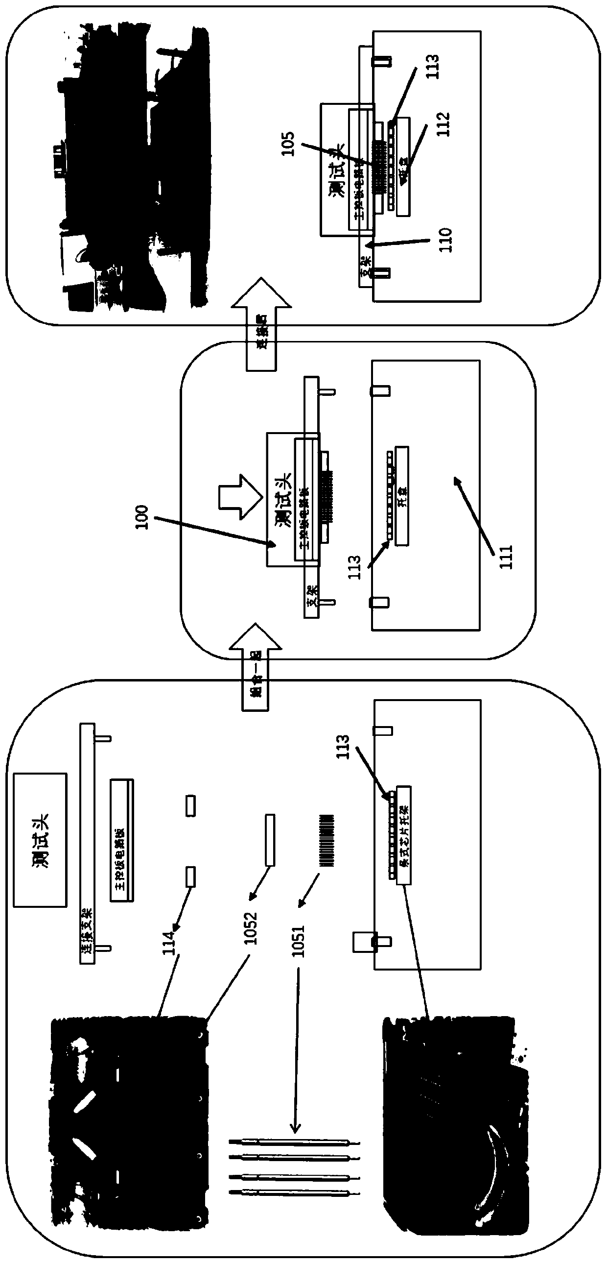
[0084] The present invention makes full use of the high-density chips on the lead frame for centralized processing, such as figure 1 As shown, after lead frame molding, plating, and baking, pre-cut ribs are performed, such as figure 2 As shown, the cutting of specific pins ensures the realization of the electrical test. Part of the chip pins of each package unit are cut and separated from the lead frame. With the unique two-dimensional identification code on the frame and the corresponding vertical and horizontal coordinates, the package unit is overall Parallel testing.

[0085] Parallel testing is implemented by connecting the chip tip to the lead frame.

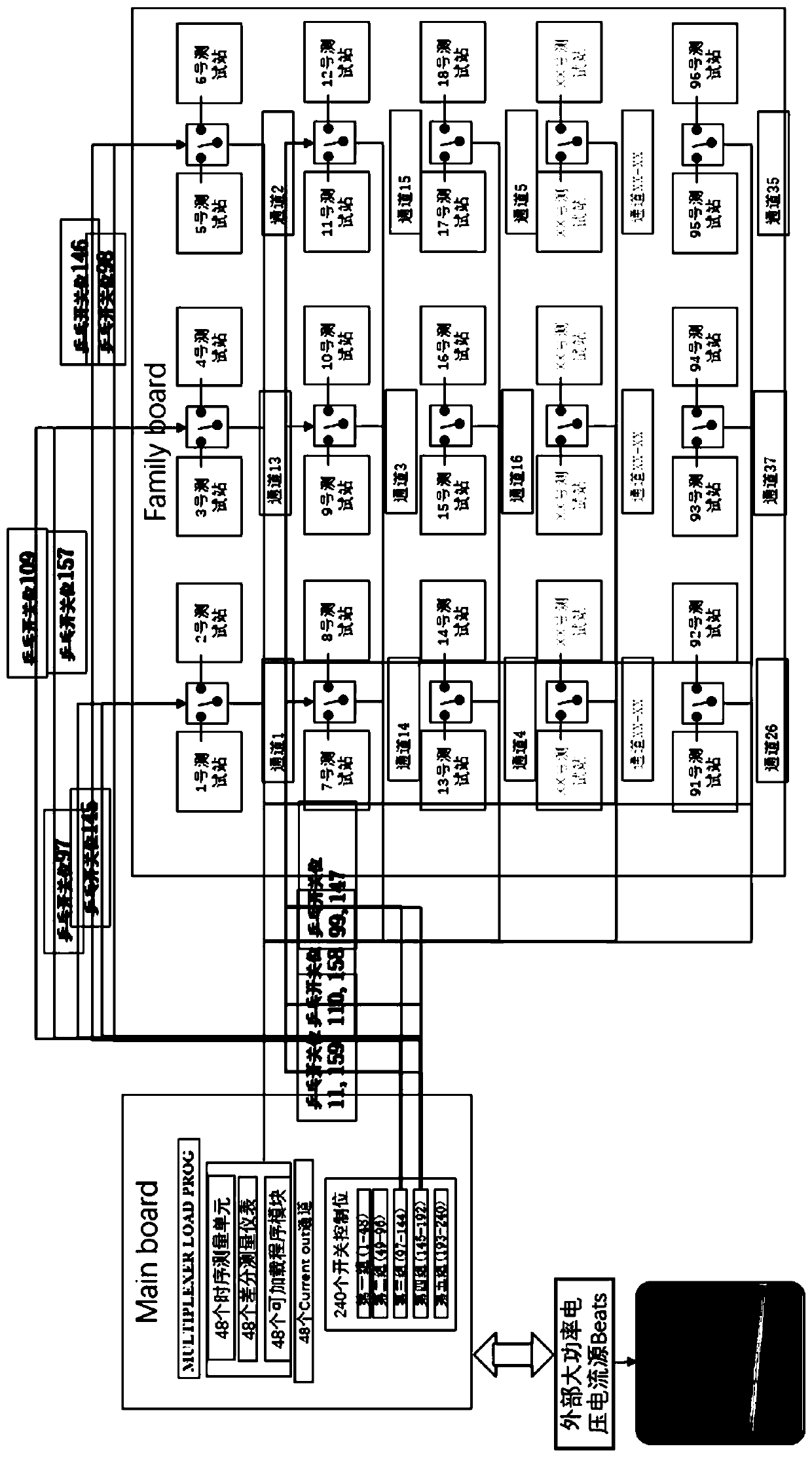
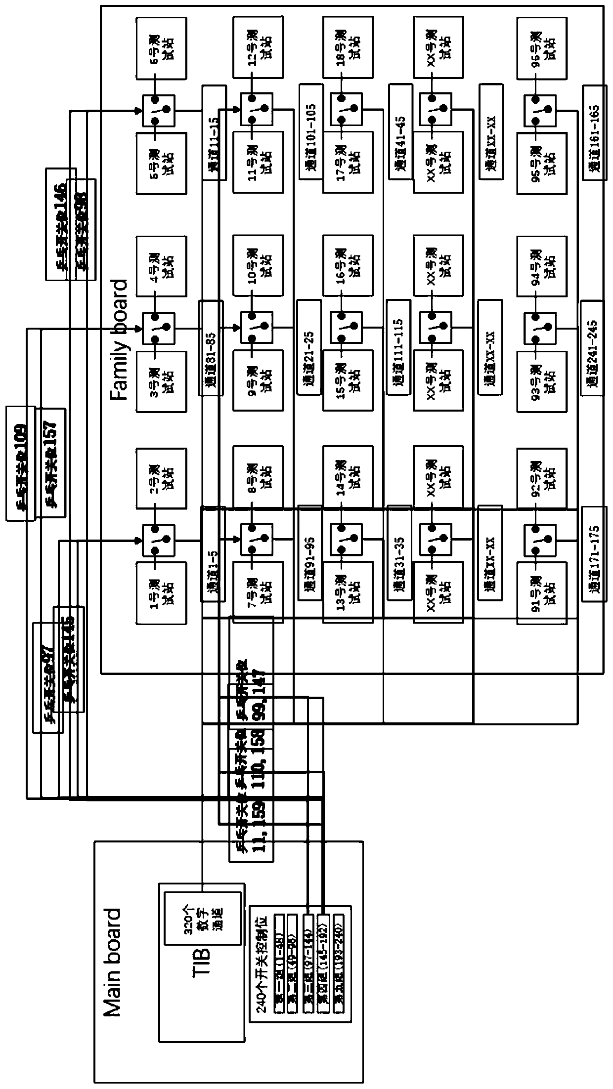
[0086] The chip packaging and testing device includes a test processing unit, a contactor support and a plurality of contactor un...


PUM


Abstract

The present invention discloses a parallel test device for a semiconductor power device which is used for measuring electrical parameters of a plurality of the semiconductor power devices in parallel.The device comprises a test head (100), a connection cable (200) and a test computer (400). The connection cable (200) and the test head (100) are in communication connection with the test computer (400). The test head (100) comprises a contact circuit board (101), a main control circuit board (102), a TIB test resource interface board (103), a programmable load loading board (104), and a probe contact device (105); and the main control circuit board (102) of the test head an control the programmable load loading board (104) through programming design to dynamically distribute the test resources; and a ping-pong test mode is employed to test the semiconductor power devices in parallel. The parallel test device for a semiconductor power device can achieve the technical effect of improvingthe test efficiency.

Description

technical field [0001] The invention relates to the technical field (H01L 21 / 66) of testing or measuring methods or equipment specially adapted for use in the manufacture or processing of semiconductor or solid state devices or parts thereof, and in particular to parallel testing equipment for semiconductor power devices. Background technique [0002] The existing traditional production process of semiconductor power devices is as follows: figure 1 Shown: [0003] The wafer is pasted on the blue film at the wafer loading station, and the entire wafer is cut into individual chips by the wafer cutting station. The pad-type solder joints on the chip are then welded and connected to the designated lead pins on the frame with high-purity metal wires at the chip bonding station, and then the overall thermal hardening and injection molding are cured, and the chip after electroplating pins are trimmed and formed Put it in the tube and then segregate and test the good product for p...

Claims


Application Information

Patent Timeline
Patent Type & Authority Applications(China)
IPC IPC(8): H01L21/66
Inventor 陈飞杨宇都俊兴周杰张震
Owner SHENZHEN STS MICROELECTRONICS
Features
  • R&D
  • Intellectual Property
  • Life Sciences
  • Materials
  • Tech Scout
  • Unparalleled Data Quality
  • Higher Quality Content
  • 60% Fewer Hallucinations
Learn More