Photolithography mask optimization design method and system

A photolithography mask and optimization design technology, applied in optics, originals for optomechanical processing, instruments, etc., can solve the problems of complicated design process, high cost, long time consumption, etc., to save design time and cost, The effect of high accuracy and simplified design steps

Pending Publication Date: 2019-05-14
CHANGXIN MEMORY TECH INC
View PDF7 Cites 0 Cited by
  • Summary
  • Abstract
  • Description
  • Claims
  • Application Information

AI Technical Summary

Problems solved by technology

[0013] In view of the above-mentioned shortcomings of the prior art, the object of the present invention is to provide a method and system for optimizing the design of a li

Method used


Image

  • Photolithography mask optimization design method and system
  • Photolithography mask optimization design method and system
  • Photolithography mask optimization design method and system

Examples


Embodiment 1

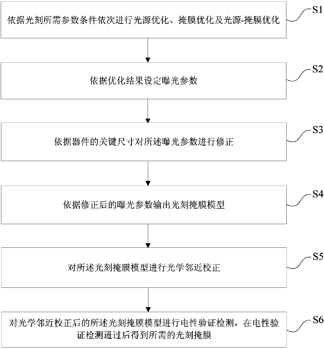
[0073] see figure 1 , the present invention provides a photolithography mask optimization design method, the photolithography mask optimization design method includes the following steps:

[0074] 1) Perform light source optimization, mask optimization, and light source-mask optimization in sequence according to the parameters required for lithography;

[0075] 2) Setting the exposure parameters according to the optimization results;

[0076] 3) Correcting the exposure parameters according to the critical dimensions of the device;

[0077] 4) Outputting the photolithographic mask model according to the corrected exposure parameters,

[0078] 5) performing optical proximity correction on the photolithography mask model; and,

[0079] 6) Carrying out an electrical verification test on the photolithography mask model after the optical proximity correction, and obtaining the required photolithography mask after the electrical verification test is passed.

[0080] As an example...

Embodiment 2

[0110] see Figure 5 , the present invention also provides a lithography mask optimization design system 2, the lithography mask optimization design system 2 is used to implement the lithography mask optimization design method as described in the first embodiment, the lithography mask Film optimization design system 2 includes: light source optimization module 20, mask optimization module 21, light source-mask optimization module 22, exposure parameter setting module 23, data storage module 24, correction module 25, model output module 26, optical proximity correction Module 27 and verification detection module 28; wherein, the light source optimization module 20 is used to optimize the light source according to the parameter conditions required by lithography; the mask optimization module 21 is used to perform mask optimization according to the parameter conditions required by lithography; The light source-mask optimization module 22 is connected to the light source optimizat...


PUM


Abstract

The invention provides a photolithography mask optimization design method and system. The photolithography mask optimization design method comprises the following steps that (1) light source optimization, mask optimization and light source-mask optimization are sequentially performed according to parameter conditions required by photolithography; (2) exposure parameters are set according to the optimization result; (3) the exposure parameters are corrected according to the key dimensions of a device; (4) a photolithography mask model is output according to the corrected exposure parameters; (5) optical proximity correction is carried out on the photolithography mask model; and (6) electrical verification detection is carried out on the photolithography mask model after optical proximity correction, and the required photolithography mask is obtained after the electrical verification detection passes. According to the photolithography mask optimization design method and system, by adopting light source optimization, mask optimization and light source-mask optimization setting exposure parameters, automatic setting of the photolithography mask can be realized, and the whole design process is relatively simple, flexible and high in accuracy.

Description

technical field [0001] The invention belongs to the field of semiconductor manufacturing, in particular to a photolithography mask optimization design method and system. Background technique [0002] In the existing semiconductor process, the design of the photolithography mask is related to the subsequent entire semiconductor process, and has a crucial impact on the manufacture of products and the yield rate of products. The existing photolithography mask design method generally includes the following steps: [0003] 1) Design photolithographic mask test patterns; [0004] 2) Photolithography mask test pattern off-line (tape out); [0005] 3) Collect key dimensions after exposure; [0006] 4) filtering and removing the collected critical dimensions to obtain the required critical dimensions; [0007] 5) Correcting the photolithographic mask model according to the obtained critical dimensions; [0008] 6) Outputting the corrected photolithography mask model; [0009] 7...

Claims


Application Information

Patent Timeline
IPC IPC(8): G03F1/36
Inventor 不公告发明人
Owner CHANGXIN MEMORY TECH INC
Why Eureka
Try Eureka