Silicon carbide MOSFET device and preparation method thereof

A silicon carbide and device technology, used in semiconductor/solid-state device manufacturing, semiconductor devices, electrical components, etc., can solve problems such as large leakage current of MOSFETs, increasing cell area of ​​silicon carbide MOSFET devices, and large Schottky contact area area. , to improve the freewheeling capacity, prevent the Schottky contact area from being too large, and reduce the production cost.

Pending Publication Date: 2019-05-14
厦门芯光润泽科技有限公司
View PDF11 Cites 5 Cited by
  • Summary
  • Abstract
  • Description
  • Claims
  • Application Information

AI Technical Summary

Problems solved by technology

[0006] However, there are still many problems in silicon carbide MOSFET devices integrating traditional junction barrier Schottky diodes, mainly in that in order to make the Schottky diodes have better freewheeling capability, a larger Schottky contact area is required
On the one hand, the larger Schottky contact area makes the MOSFET have a larger leakage current when it works normally, on the other hand, it also increases the cell area of ​​the silicon carbide MOSFET device, which increases the cost of chip preparation

Method used


Image

  • Silicon carbide MOSFET device and preparation method thereof
  • Silicon carbide MOSFET device and preparation method thereof
  • Silicon carbide MOSFET device and preparation method thereof

Examples


Embodiment 1

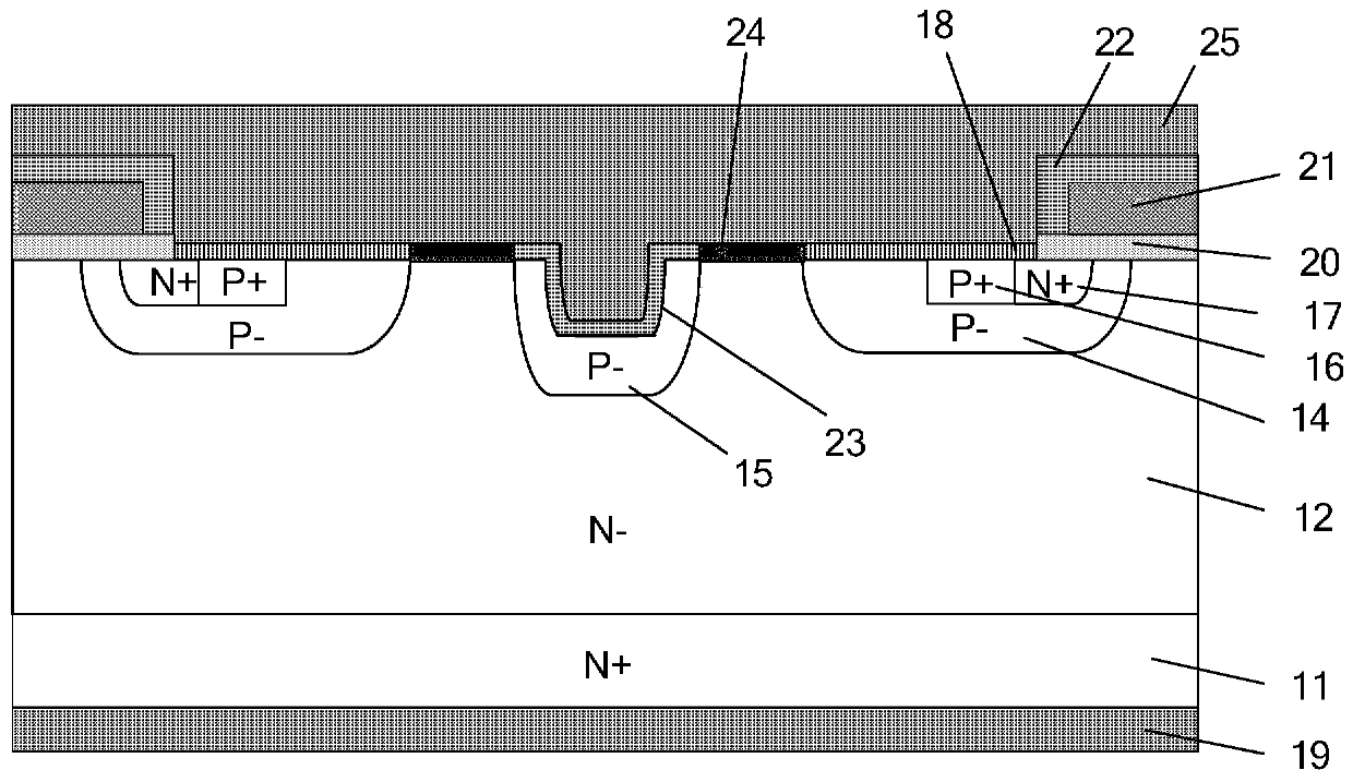
[0052] This embodiment provides a silicon carbide MOSFET device integrating a trench junction barrier Schottky diode, and its structural cross-sectional schematic diagram is as follows figure 1 shown.

[0053] The device includes a drain electrode from bottom to top (the drain electrode includes figure 1 Metal shown in 19), N+ substrate 11 and N- epitaxial layer 12. The N-epitaxial layer 12 has a first P-well region 14, and the first P-well region 14 has a P+ region 16 and an N+ region 17 (the depth of the first P-well region 14 is greater than the depth of the N+ region 17 and the P+ region 16). The number of the first P-well region 14 is more than two, and usually can be more.

[0054] The device further includes: a first metal 18 forming a first ohmic contact with the upper surface of the P+ region 16 and part of the upper surface of the N+ region 17 . In addition, the first metal 18 also forms a corresponding good ohmic contact with the upper surface of part of the firs...

Embodiment 2

[0083] This embodiment provides a silicon carbide MOSFET device integrating a trench junction barrier Schottky diode, and its structural cross-sectional schematic diagram is as follows Figure 7 shown.

[0084] The device includes a drain electrode from bottom to top (the drain electrode includes Figure 7 Metal 39 shown in), N+ substrate 31 and N- epitaxial layer 32; N- epitaxial layer 32 has a first P- well region 34, and there are P+ region 36 and N+ region 37 in the first P-well region 34 ( At this time, the depth of the first P-well region 34 is greater than the depth of the N+ region 37 and the P+ region 36). The number of the first P-well regions 34 is more than two.

[0085] The device also includes: a first metal 38, the first metal 38 forms a first ohmic contact with the upper surface of the P+ region 36 and part of the upper surface of the N+ region 37 (the first metal 38 also covers part of the first P- well region 34 upper surface, but the contact between them ...


PUM

PropertyMeasurementUnit
depthaaaaaaaaaa
widthaaaaaaaaaa
thicknessaaaaaaaaaa

Abstract

The invention discloses a silicon carbide MOSFET device and a preparation method thereof. The silicon carbide MOSFET device comprises, form bottom to top, a leakage electrode, a N+substrate and N-epitaxial layer. The N-epitaxial layer is provided with first P-well areas, a first metal, second well areas and a second metal. The first P-well areas are provided with P+areas and N+areas; first ohmic contact is formed by the first metal, the upper surfaces of the P+areas and part of the upper surfaces of the N+areas; the second P-well areas are arranged between every two adjacent first P-well areas, the second P-well areas and the first P-well areas arranged on two side of the second P-well areas are all provided with first gaps, and grooves are encircled by the second P-well areas; and the second metal covers the surface of the groove to form second ohmic contact and the upper surface of the first gap to form Schottky contact. According to the silicon carbide MOSFET device, the flow-continuing ability is improved, and meanwhile the problem that the leakage current of the Schottky contact area in a high-pressure blockage mode is too large is solved.

Description

technical field [0001] The invention relates to the field of semiconductors, in particular to a silicon carbide MOSFET device and a preparation method thereof. Background technique [0002] In recent years, with the continuous development of power electronic systems, higher requirements have been placed on the power devices in the system. Silicon (Si)-based power electronic devices have been unable to meet the requirements of system applications due to the limitations of the material itself. [0003] As a representative of the third-generation semiconductor material, silicon carbide (SiC) material is far better than silicon material in many characteristics. As a commercialized device in recent years, silicon carbide MOSFET devices have great potential to replace existing IGBTs in terms of on-resistance, switching time, switching loss and heat dissipation performance. [0004] However, due to the large bandgap of silicon carbide materials, the turn-on voltage of the parasit...

Claims


Application Information

Patent Timeline
Patent Type & Authority Applications(China)
IPC IPC(8): H01L29/78H01L21/04
Inventor 卓廷厚李钊君刘延聪
Owner 厦门芯光润泽科技有限公司
Why Eureka
Try Eureka