A low stress passivated mesa-type extended wavelength indium gallium arsenide detector preparation method

A detector and table-top technology, which is applied in the field of infrared detector preparation, can solve the problems of large warpage of large area array detector chips, poor reliability of large area array detector chips, unfavorable short-wave infrared focal plane connectivity rate and the like. , to achieve good passivation effect, reduce dangling keys, and achieve the effect of high reliability

Active Publication Date: 2021-04-09
SHANGHAI INST OF TECHNICAL PHYSICS - CHINESE ACAD OF SCI
View PDF3 Cites 0 Cited by
  • Summary
  • Abstract
  • Description
  • Claims
  • Application Information

AI Technical Summary

Problems solved by technology

[0013] In the existing manufacturing process of the mesa-type InGaAs focal plane detector chip, the conventional inductively coupled plasma chemical vapor deposition growth passivation film has a large warpage of the large area detector chip due to the high stress of the film. , which is not conducive to the control of the connectivity rate of the short-wave infrared focal plane flip welding process; and due to the high stress of the film, the reliability of the film is poor, and the subsequent heat treatment process will easily cause the surface of the film to bubble and fall off, resulting in poor reliability of the large area detector chip

Method used


Image

  • A low stress passivated mesa-type extended wavelength indium gallium arsenide detector preparation method
  • A low stress passivated mesa-type extended wavelength indium gallium arsenide detector preparation method

Examples


Embodiment 1

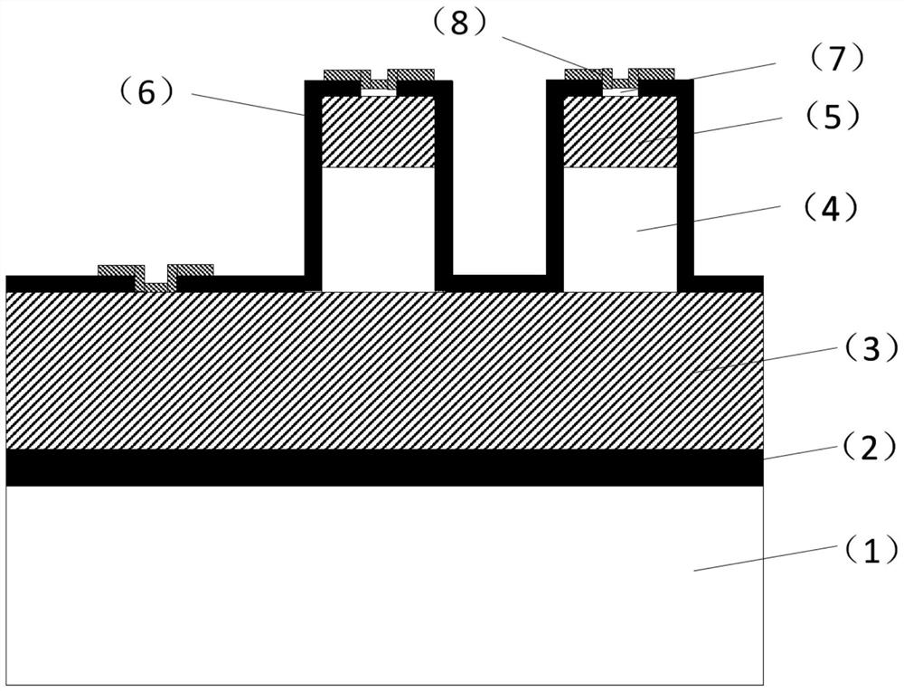
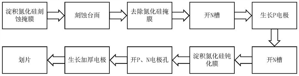
[0047] 1 Deposit silicon nitride etching mask, used as an etching mask, using plasma enhanced chemical vapor deposition (PECVD) technology to deposit silicon nitride with a thickness of 400±20nm, RF power of 40±5W, substrate Bottom temperature 330±5℃, gas flow SiH 4 :N 2is 1:18;

[0048] 2 Etching the mesa is divided into two parts: etching silicon nitride and etching InGaAs epitaxial material to form the mesa. Silicon nitride is etched using inductively coupled plasma (ICP) etching technology. The etching conditions are: ICP power is 2000±5W, RF power is 40±5W, and SF is used. 6 As an etching gas; use inductively coupled plasma (ICP) etching technology to etch the mesa, the etching conditions are: ICP power is 350±5W, RF power is 130±5W, using Cl 2 and N 2 as an etching gas;

[0049] 3 Remove the silicon nitride mask, use hydrofluoric acid buffer solution to etch at room temperature for 120±5s, and the volume ratio of the etching solution is HF:NH 4 F:H 2 O is 3:6:10; ...

Embodiment 2

[0058] 1 Deposit silicon nitride etching mask, used as an etching mask, using plasma enhanced chemical vapor deposition (PECVD) technology to deposit silicon nitride with a thickness of 400±20nm, RF power of 40±5W, substrate Bottom temperature 330±5℃, gas flow SiH 4 :N 2 is 1:18;

[0059] 2 Etching the mesa is divided into two parts: etching silicon nitride and etching InGaAs epitaxial material to form the mesa. Silicon nitride is etched using inductively coupled plasma (ICP) etching technology. The etching conditions are: ICP power is 2000±5W, RF power is 40±5W, and SF is used. 6 As an etching gas; use inductively coupled plasma (ICP) etching technology to etch the mesa, the etching conditions are: ICP power is 350±5W, RF power is 130±5W, using Cl 2 and N 2 as an etching gas;

[0060] 3 Remove the silicon nitride mask, use hydrofluoric acid buffer solution to etch at room temperature for 120±5s, and the volume ratio of the etching solution is HF:NH 4 F:H 2 O is 3:6:10;...

Embodiment 3

[0069] 1 Deposit silicon nitride etching mask, used as an etching mask, using plasma enhanced chemical vapor deposition (PECVD) technology to deposit silicon nitride with a thickness of 400±20nm, RF power of 40±5W, substrate Bottom temperature 330±5℃, gas flow SiH 4 :N 2 is 1:18;

[0070] 2 Etching the mesa is divided into two parts: etching silicon nitride and etching InGaAs epitaxial material to form the mesa. Silicon nitride is etched using inductively coupled plasma (ICP) etching technology. The etching conditions are: ICP power is 2000±5W, RF power is 40±5W, and SF is used. 6 As an etching gas; use inductively coupled plasma (ICP) etching technology to etch the mesa, the etching conditions are: ICP power is 350±5W, RF power is 130±5W, using Cl 2 and N 2 as an etching gas;

[0071] 3 Remove the silicon nitride mask, use hydrofluoric acid buffer solution to etch at room temperature for 120±5s, and the volume ratio of the etching solution is HF:NH 4 F:H 2 O is 3:6:10;...


PUM


Abstract

The invention discloses a preparation method of a mesa-type extended-wavelength InGaAs detector with low stress passivation. The structure is as follows: on a semi-insulating InP substrate, N + type InP layer, composition graded N + Type In x Al 1‑x As buffer layer, In x Ga 1‑x As absorbing layer, P + Type In x Al 1‑x As cap layer, silicon nitride SiN x Passivation film, P electrode, thickened electrode. The passivation film is a low-stress silicon nitride passivation film grown by inductively coupled plasma chemical vapor deposition technology. The invention has the advantages of: adopting low-stress silicon nitride film passivation, controlling the warpage of the large area array detector chip to be less than 10 μm, which is conducive to the realization of focal plane devices with low blind element rate; low-stress silicon nitride passivation The reliability of the film is high; the surface side passivation effect of the low-stress silicon nitride passivation film is good.

Description

technical field [0001] The invention relates to the preparation technology of infrared detectors, in particular to a preparation method of low-stress passivated mesa-type extended-wavelength indium gallium arsenic detectors, which is suitable for preparing large arrays, small pixels, high aspect ratios, and high sensitivity , High reliability mesa InGaAs detector. Background technique [0002] The short-wave infrared InGaAs detector has excellent performances such as high detection rate, high quantum efficiency, and near-room temperature operation. With the increase of indium composition, the cut-off wavelength of the extended-wavelength InGaAs detector can be extended from 1.7 μm to 2.5 μm. It has wide application value in environmental monitoring, spectroscopy, night vision, etc. With the demand for high-resolution development of short-wave infrared imaging technology, extended-wavelength InGaAs focal plane detectors are developing in the direction of large-scale, small p...

Claims


Application Information

Patent Timeline
Patent Type & Authority Patents(China)
IPC IPC(8): H01L31/18H01L31/105C23C16/513C23C16/34
CPCY02P70/50
Inventor 万露红邵秀梅李雪邓双燕曹高奇程吉凤
Owner SHANGHAI INST OF TECHNICAL PHYSICS - CHINESE ACAD OF SCI
Why Eureka
Try Eureka