LED packaging structure and method

A technology of LED packaging and LED chips, applied in the direction of electrical components, circuits, semiconductor devices, etc., can solve the problems of peeling of plastic packaging materials, affecting the sealing of packaging, peeling of plastic packaging materials and substrates, etc., and achieve the effect of reducing stress

Active Publication Date: 2019-05-21
南通沃特光电科技有限公司
View PDF4 Cites 6 Cited by
  • Summary
  • Abstract
  • Description
  • Claims
  • Application Information

AI Technical Summary

Problems solved by technology

[0002] Most of the existing LED chip packages are of COB structure. As the heat of the LED chip increases during preparation or use, the plastic packaging material will expand or shrink and the substrate will generate greater stress due to different thermal expansion coefficients, which will lead to The peeling of the molding compound and the substrate affects the sealing of the package and may cause the peeling of the molding compound

Method used


Image

  • LED packaging structure and method
  • LED packaging structure and method
  • LED packaging structure and method

Examples


Embodiment Construction

[0033] The idea of ​​the present invention is to design an LED chip package that enhances heat dissipation and prevents warping and peeling off, and specific embodiments will be described in the following content.

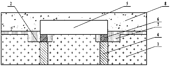
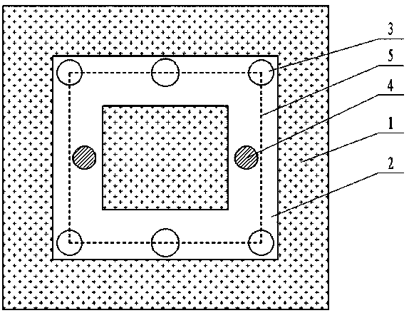
[0034] see figure 1 and 2 , LED encapsulation structure of the present invention, it comprises:

[0035] A heat dissipation substrate 1, the heat dissipation substrate 1 is provided with an annular groove 2, and a plurality of through holes 3 passing through the heat dissipation substrate 1 are arranged at the bottom of the annular groove 2, and the plurality of through holes 3 A part of the through hole is filled with conductive material to form the conductive hole 4; this part of the through hole realizes the function of a conductive path, which should correspond to the position of the electrode of the LED chip.

[0036] The LED chip 5 is flip-mounted on the conductive hole 4 via the solder ball 6 so that the bottom surface of the LED chip 5 contacts the heat d...


PUM


Abstract

The invention provides an LED packaging structure and method. The LED packaging structure comprises a polymer layer and a fluorescent resin layer covering the polymer layer and the LED chip; the polymer layer is a photo-curable and heat-curable polymer material; the fluorescent resin layer is a thermosetting resin material; and the final curing of the polymer layer is realized in the same heatingstep together with the curing of the fluorescent resin layer.

Description

technical field [0001] The invention relates to the field of semiconductor device packaging, belongs to the classification number H01L33 / 00, and specifically relates to an LED packaging structure and a packaging method thereof. Background technique [0002] Most of the existing LED chip packages are of COB structure. As the heat of the LED chip increases during preparation or use, the plastic packaging material will expand or shrink and the substrate will generate greater stress due to different thermal expansion coefficients, which will lead to The peeling of the molding compound from the substrate affects the sealing performance of the package and may cause the peeling of the molding compound. Contents of the invention [0003] Based on solving the above problems, the present invention provides a LED packaging structure, which includes: [0004] A heat dissipation substrate, the heat dissipation substrate is provided with an annular groove, and a plurality of through ho...

Claims


Application Information

Patent Timeline
IPC IPC(8): H01L33/54H01L33/56H01L33/50H01L33/64
Inventor 钱畅
Owner 南通沃特光电科技有限公司
Why Eureka
Try Eureka